UMF9NTR Rohm Semiconductor, UMF9NTR Datasheet - Page 2
UMF9NTR
Manufacturer Part Number
UMF9NTR
Description
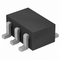
TRANS NPN/N-CH 12V 500MA SOT-363
Manufacturer
Rohm Semiconductor
Datasheet
1.UMF9NTR.pdf
(6 pages)
Specifications of UMF9NTR
Transistor Type
NPN, N-Channel
Applications
General Purpose
Voltage - Rated
12V NPN, 30V N-Channel
Current Rating
500mA NPN, 100mA N-Channel
Mounting Type
Surface Mount
Package / Case
6-TSSOP, SC-88, SOT-363
Module Configuration
Dual
Transistor Polarity
NPN + N MOSFET
Collector Emitter Voltage V(br)ceo
12V
Gain Bandwidth Ft Typ
320MHz
Power Dissipation Pd
150mW
Dc Collector Current
500mA
Operating
RoHS Compliant
Dc Current Gain Hfe
270
Rohs Compliant
Yes
Lead Free Status / RoHS Status
Lead free / RoHS Compliant
Available stocks
Company
Part Number
Manufacturer
Quantity
Price
Company:

Part Number:
UMF9NTR
Manufacturer:
ROHM
Quantity:
3 432


Transistors
Tr1
Tr2
Tr1
Tr2
∗1 P
∗2 120mW per element must not be exceeded. Each terminal mounted on a recommended land.
∗1 Single pulse P
∗2 120mW per element must not be exceeded. Each terminal mounted on a recommended land.
Collector-base voltage
Collector-emitter voltage
Emitter-base voltage
Collector current
Power dissipation
Junction temperature
Range of storage temperature
Drain-source voltage
Gate-source voltage
Drain current
Reverse drain
current
Total power dissipation
Channel temperature
Range of storage temperature
Collector-emitter breakdown voltage
Emitter-base breakdown voltage
Collector cut-off current
Emitter cut-off current
Collector-emitter saturation voltage
DC current gain
Collector output capacitance
Gate-source leakage
Drain-source breakdown voltage
Zero gate voltage drain current
Gate-threshold voltage
Static drain-source
Forward transfer admittance
Output capacitance
Reverce transfer capacitance
Turn-on delay time
Turn-off delay time
Fall time
Collector-base breakdown voltage
Transition frequency
Input capacitance
Rise time
Electrical characteristics (Ta=25°C)
Absolute maximum ratings (Ta=25°C)
W
on-state resistance
≤10ms Duty cycle≤50%
Parameter
Parameter
W
Parameter
Parameter
=1ms
Continuous
Continuous
Pulsed
Pulsed
Symbol
Symbol
V
V
V
V
Tstg
V
Tstg
I
Tch
I
I
P
I
DRP
P
Tj
CBO
CEO
EBO
I
DSS
GSS
I
DR
CP
DP
C
D
C
D
Symbol
V
Symbol
V
R
BV
BV
BV
V
150(TOTAL)
150(TOTAL)
(BR)DSS
−55
−55
Cob
t
t
I
I
I
|Y
C
CE(sat)
I
C
C
h
GS(th)
DS(on)
d(on)
d(off)
CBO
EBO
GSS
DSS
f
t
t
FE
oss
CEO
CBO
T
rss
EBO
iss
fs
r
f
Limits
Limits
|
500
150
±20
100
200
100
200
150
1.0
to
to
15
12
30
6
+150
+150
Min.
Min.
270
0.8
12
15
30
20
6
−
−
−
−
−
−
−
−
−
−
−
−
−
−
−
−
Unit
mW
Unit
mW
mA
mA
mA
mA
mA
°C
°C
°C
°C
V
V
V
A
V
V
Typ.
Typ.
100
320
∗1
∗2
∗1
∗1
∗2
7.5
13
15
35
80
80
−
−
−
−
−
−
−
−
−
−
5
7
−
9
4
Max.
Max.
100
100
250
680
1.0
1.5
±1
13
−
−
−
−
−
−
8
−
−
−
−
−
−
−
−
MHz
Unit
Unit
mV
nA
nA
pF
µA
µA
ms
pF
pF
pF
ns
ns
ns
ns
V
V
V
V
Ω
Ω
−
V
I
I
I
V
V
I
V
V
V
V
I
V
V
I
I
V
V
I
V
R
C
C
E
C
D
D
D
D
CB
EB
CE
CE
CB
GS
DS
DS
DS
DS
GS
=1mA
=10µA
=10µA
=200mA, I
GS
=10µA, V
=10mA, V
=1mA, V
=10mA, V
=6V
=15V
=2V, I
=2V, I
=10V, I
=30V, V
=3V, I
=3V, I
=5V, V
=±20V, V
=5V, R
=10Ω
C
E
D
D
=−10mA, f=100MHz
GS
GS
=10mA
=100µA
=10mA
L
E
GS
Conditions
Conditions
=500Ω,
=0mA, f=1MHz
GS
GS
DD
B
=2.5V
=0V, f=1MHz
=10mA
DS
=0V
=0V
=4V
=0V
5V,
Rev.A
UMF9N
2/5
Related parts for UMF9NTR
Image
Part Number
Description
Manufacturer
Datasheet
Request
R

Part Number:
Description:
Manufacturer:
Rohm Semiconductor
Datasheet:
Part Number:
Description:
Manufacturer:
Rohm Semiconductor
Datasheet:
Part Number:
Description:
Manufacturer:
Rohm Semiconductor
Datasheet:
Part Number:
Description:
Manufacturer:
Rohm Semiconductor
Datasheet:
Part Number:
Description:
Manufacturer:
Rohm Semiconductor
Datasheet:
Part Number:
Description:
Manufacturer:
Rohm Semiconductor
Datasheet:
Part Number:
Description:
Manufacturer:
Rohm Semiconductor
Datasheet:
Part Number:
Description:
Manufacturer:
Rohm Semiconductor
Datasheet:
Part Number:
Description:
Manufacturer:
Rohm Semiconductor
Datasheet:
Part Number:
Description:
Manufacturer:
Rohm Semiconductor
Datasheet:
Part Number:
Description:
Manufacturer:
Rohm Semiconductor
Datasheet:
Part Number:
Description:
Manufacturer:
Rohm Semiconductor
Datasheet:

Part Number:
Description:
DIODE SWITCH 80V 25MA SMD5 TR
Manufacturer:
Rohm Semiconductor
Datasheet: