2N4401RLRM ON Semiconductor, 2N4401RLRM Datasheet

TRANS SS NPN GP 40V 600MA TO-92

2N4401RLRM

Manufacturer Part Number
2N4401RLRM
Description
TRANS SS NPN GP 40V 600MA TO-92
Manufacturer
ON Semiconductor
Datasheet

Specifications of 2N4401RLRM

Transistor Type
NPN
Current - Collector (ic) (max)
600mA
Voltage - Collector Emitter Breakdown (max)
40V
Vce Saturation (max) @ Ib, Ic
750mV @ 50mA, 500mA
Dc Current Gain (hfe) (min) @ Ic, Vce
100 @ 150mA, 1V
Power - Max
625mW
Frequency - Transition
250MHz
Mounting Type
Through Hole
Package / Case
TO-92-3 (Standard Body), TO-226
Lead Free Status / RoHS Status
Contains lead / RoHS non-compliant
Current - Collector Cutoff (max)
-
2N4401
General Purpose
Transistors
NPN Silicon
Features
Maximum ratings are those values beyond which device damage can occur.
Maximum ratings applied to the device are individual stress limit values (not normal
operating conditions) and are not valid simultaneously. If these limits are exceeded,
device functional operation is not implied, damage may occur and reliability may
be affected.
*For additional information on our Pb−Free strategy and soldering details, please
MAXIMUM RATINGS
THERMAL CHARACTERISTICS
© Semiconductor Components Industries, LLC, 2005
August, 2005 − Rev. 2
download the ON Semiconductor Soldering and Mounting Techniques Reference
Manual, SOLDERRM/D.
Thermal Resistance, Junction−to−Ambient
Thermal Resistance, Junction−to−Case
Collector − Emitter Voltage
Collector − Base Voltage
Emitter − Base Voltage
Collector Current − Continuous
Total Device Dissipation
Operating and Storage Junction
Pb−Free Packages are Available*
@ T
Derate above 25°C
@ T
Derate above 25°C
Temperature Range
A
C
= 25°C
= 25°C
Characteristic
Rating
Preferred Device
Symbol
Symbol
T
V
V
V
R
R
J
P
P
, T
CEO
CBO
EBO
I
qJA
qJC
C
D
D
stg
−55 to
Value
+150
Max
83.3
600
625
200
6.0
5.0
1.5
40
60
12
1
mW/°C
mW/°C
mAdc
°C/W
°C/W
Unit
Unit
Vdc
Vdc
Vdc
mW
°C
W
See detailed ordering and shipping information in the package
dimensions section on page 3 of this data sheet.
Preferred devices are recommended choices for future use
and best overall value.
(Note: Microdot may be in either location)
1
2
2N4401 = Device Code
A
Y
WW
G
ORDERING INFORMATION
3
MARKING DIAGRAM
http://onsemi.com
BASE
2
= Assembly Location
= Year
= Work Week
= Pb−Free Package
AYWW G
4401
COLLECTOR
2N
G
Publication Order Number:
EMITTER
3
CASE 29
STYLE 1
1
TO−92
2N4401/D

Related parts for 2N4401RLRM

2N4401RLRM Summary of contents

Page 1

... Pb−Free strategy and soldering details, please download the ON Semiconductor Soldering and Mounting Techniques Reference Manual, SOLDERRM/D. © Semiconductor Components Industries, LLC, 2005 August, 2005 − Rev. 2 ...

Page 2

ELECTRICAL CHARACTERISTICS Characteristic OFF CHARACTERISTICS Collector−Emitter Breakdown Voltage (Note 1.0 mAdc Collector−Base Breakdown Voltage (I = 0.1 mAdc Emitter−Base Breakdown Voltage (I = 0.1 mAdc ...

Page 3

... ORDERING INFORMATION Device 2N4401 2N4401G 2N4401RLRA 2N4401RLRAG 2N4401RLRM 2N4401RLRMG 2N4401RLRP 2N4401RLRPG †For information on tape and reel specifications, including part orientation and tape sizes, please refer to our Tape and Reel Packaging Specifications Brochure, BRD8011/D. SWITCHING TIME EQUIVALENT TEST CIRCUITS 1.0 to 100 ms, DUTY CYCLE ≈ ...

Page 4

I , COLLECTOR CURRENT (mA) C Figure 5. Turn−On Time 300 200 100 ...

Page 5

This group of graphs illustrates the relationship between h and other “h” parameters for this series of transistors obtain these curves, a high−gain and a low−gain unit were 300 200 100 0.1 0.2 0.3 ...

Page 6

1.0 0.7 0.5 0.3 0.2 0.1 0.2 0.3 0.5 0.7 1.0 1.0 0 0.4 0.2 0 0.01 0.02 0.03 0.05 ...
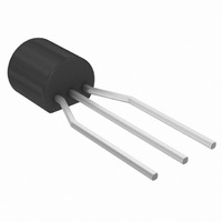
Page 7

... CASE 29−11 ISSUE SECTION X−X N. American Technical Support: 800−282−9855 Toll Free USA/Canada Japan: ON Semiconductor, Japan Customer Focus Center 2−9−1 Kamimeguro, Meguro−ku, Tokyo, Japan 153−0051 Phone: 81−3−5773−3850 http://onsemi.com 7 NOTES: 1. DIMENSIONING AND TOLERANCING PER ANSI Y14 ...

Related keywords