MJE18002 ON Semiconductor, MJE18002 Datasheet
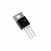
TRANS PWR NPN 2A 450V TO220AB

MJE18002

Manufacturer Part Number
MJE18002
Description
TRANS PWR NPN 2A 450V TO220AB
Manufacturer
ON Semiconductor
Series
SWITCHMODE™r
Datasheet

Specifications of MJE18002

Transistor Type
NPN
Current - Collector (ic) (max)
2A
Voltage - Collector Emitter Breakdown (max)
450V
Vce Saturation (max) @ Ib, Ic
500mV @ 200mA, 1A
Current - Collector Cutoff (max)
100µA
Dc Current Gain (hfe) (min) @ Ic, Vce
14 @ 200mA, 5V
Power - Max
50W
Frequency - Transition
13MHz
Mounting Type
Through Hole
Package / Case
TO-220-3 (Straight Leads)
Lead Free Status / RoHS Status
Contains lead / RoHS non-compliant
Other names
MJE18002OS

Available stocks

Company
Part Number
Manufacturer
Quantity
Price
Part Number:
MJE18002
Manufacturer:
ON
Quantity:
637
Part Number:
MJE18002G
Manufacturer:
NEC
Quantity:
6 144
MJE18002G
SWITCHMODEt
NPN Bipolar Power Transistor
For Switching Power Supply Applications
designed for use in 220 V line operated Switchmode Power supplies
and electronic light ballasts.
Features
Stresses exceeding Maximum Ratings may damage the device. Maximum
Ratings are stress ratings only. Functional operation above the Recommended
Operating Conditions is not implied. Extended exposure to stresses above the
Recommended Operating Conditions may affect device reliability.
1. Pulse Test: Pulse Width = 5 ms, Duty Cycle ≤ 10%.
*For additional information on our Pb−Free strategy and soldering details, please
MAXIMUM RATINGS
THERMAL CHARACTERISTICS
© Semiconductor Components Industries, LLC, 2010
April, 2010 − Rev. 7
download the ON Semiconductor Soldering and Mounting Techniques
Reference Manual, SOLDERRM/D.
Collector−Emitter Sustaining Voltage
Collector−Emitter Breakdown Voltage
Emitter−Base Voltage
Collector Current
Base Current
Total Device Dissipation @ T
Derate above 25°C
Operating and Storage Temperature
Thermal Resistance, Junction−to−Case
Thermal Resistance, Junction−to−Ambient
Maximum Lead Temperature for Soldering
Purposes 1/8″ from Case for 5 Seconds
The MJE18002G have an applications specific state−of−the−art die
Improved Efficiency Due to Low Base Drive Requirements:
Tight Parametric Distributions are Consistent Lot−to−Lot
Standard TO−220
These Devices are Pb−Free and are RoHS Compliant*
High and Flat DC Current Gain h
Fast Switching
No Coil Required in Base Circuit for Turn−Off (No Current Tail)
Characteristics
Rating
− Continuous
− Peak (Note 1)
− Continuous
− Peak (Note 1)
C
= 25_C
FE
Symbol
Symbol
T
V
V
V
R
R
J
I
I
P
CEO
EBO
, T
T
CES
CM
BM
I
I
qJC
qJA
C
B
D
L
stg
−65 to 150
Value
1000
Max
62.5
450
260
9.0
2.0
5.0
1.0
2.0
0.4
2.5
50
1
W/_C
_C/W
_C/W
Unit
Unit
Vdc
Vdc
Vdc
Adc
Adc
_C
_C
W
MJE18002G
Device
100 VOLTS − 50 WATTS
POWER TRANSISTOR
1
ORDERING INFORMATION
2
A
Y
WW = Work Week
G
3
MARKING DIAGRAM
2.0 AMPERES
http://onsemi.com
= Assembly Location
= Year
= Pb−Free Package
(Pb−Free)
MJE18002G
Package
TO−220
AY WW
CASE 221A−09
Publication Order Number:
TO−220AB
STYLE 1
50 Units / Rail
Shipping
MJE18002/D

Related parts for MJE18002

MJE18002 Summary of contents

Page 1

... MJE18002G SWITCHMODEt NPN Bipolar Power Transistor For Switching Power Supply Applications The MJE18002G have an applications specific state−of−the−art die designed for use in 220 V line operated Switchmode Power supplies and electronic light ballasts. Features • Improved Efficiency Due to Low Base Drive Requirements: High and Flat DC Current Gain h ♦ ...

Page 2

ELECTRICAL CHARACTERISTICS Characteristic OFF CHARACTERISTICS Collector−Emitter Sustaining Voltage (I C Collector Cutoff Current (V = Rated V CE Collector Cutoff Current (V = Rated V CE Collector Cutoff Current (V = 800 Emitter Cutoff Current (V = ...

Page 3

ELECTRICAL CHARACTERISTICS − continued (T Characteristic SWITCHING CHARACTERISTICS: Resistive Load (D.C. ≤ 10%, Pulse Width = 20 ms) Turn−On Time I = 0.4 Adc mAdc 0.2 Adc B2 Turn−Off Time V = 300 ...

Page 4

T = 125° 25° 0.01 0.10 1.00 0.01 0. COLLECTOR CURRENT (AMPS) C Figure 1. DC Current Gain @ 1 Volt 25° 0.4 A ...

Page 5

TYPICAL SWITCHING CHARACTERISTICS 2500 B(off 300 V 2000 1500 1000 500 0 0.4 0.6 0.8 1.0 ...

Page 6

... T = 25° 125° FORCED GAIN FE Figure 13. Inductive Fall Time GUARANTEED SAFE OPERATING AREA INFORMATION 10. (MJE18002) 1.00 0.10 0.01 10 100 10 100 V , COLLECTOR-EMITTER VOLTAGE (VOLTS) CE Figure 15. Forward Bias Safe Operating Area 1.0 0.8 0.6 0.4 THERMAL 0.2 DERATING 0 100 100 T , CASE TEMPERATURE (°C) C Figure 17 ...

Page 7

... Figure 19. Inductive Switching Measurements 100 mF MTP8P10 V MTP8P10 CE Rb1 MUR105 I I out B A Rb2 MJE210 V(BR)CEO(sus) MTP12N10 RB2 = ∞ VOLTS CC I (pk) = 100 TYPICAL THERMAL RESPONSE P (pk DUTY CYCLE 1.00 10.00 t, TIME (ms) (t)) for MJE18002 qJC http://onsemi.com 10% V CLAMP 90 TIME I PEAK C V PEAK ...

Page 8

... S 0.045 0.055 1.15 1.39 T 0.235 0.255 5.97 6.47 U 0.000 0.050 0.00 1.27 V 0.045 --- 1.15 --- Z --- 0.080 --- 2.04 PIN 1. BASE 2. COLLECTOR 3. EMITTER 4. COLLECTOR ON Semiconductor Website: www.onsemi.com Order Literature: http://www.onsemi.com/orderlit For additional information, please contact your local Sales Representative MJE18002/D ...

Related keywords