NSS40600CF8T1G ON Semiconductor, NSS40600CF8T1G Datasheet
NSS40600CF8T1G
Specifications of NSS40600CF8T1G
Available stocks


Related parts for NSS40600CF8T1G

NSS40600CF8T1G Summary of contents
Page 1
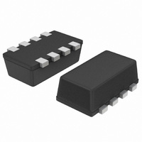
... PIN CONNECTIONS ORDERING INFORMATION Device Package Shipping NSS40600CF8T1G ChipFET 3000/ (Pb−Free) Tape & Reel †For information on tape and reel specifications, including part orientation and tape sizes, please refer to our Tape and Reel Packaging Specifications Brochure, BRD8011/D. Publication Order Number: NSS40600CF8/D † ...
Page 2
ELECTRICAL CHARACTERISTICS Characteristic OFF CHARACTERISTICS Collector −Emitter Breakdown Voltage (I = −10 mAdc Collector −Base Breakdown Voltage (I = −0.1 mAdc Emitter −Base Breakdown Voltage (I = −0.1 mAdc, I ...
Page 3
0.20 0.15 0.10 0.05 0 0.001 0.01 0 COLLECTOR CURRENT (A) C Figure 1. Collector Emitter Saturation Voltage vs. Collector Current 750 150° 650 550 150° 450 ...
Page 4
V , EMITTER BASE VOLTAGE (V) EB Figure 7. Input Capacitance 10 1.0 0.1 0.01 0.01 225 C (pF) ibo 200 175 150 125 100 75 ...
Page 5
... SCALE 20:1 inches *For additional information on our Pb−Free strategy and soldering details, please download the ON Semiconductor Soldering and Mounting Techniques Reference Manual, SOLDERRM/D. N. American Technical Support: 800−282−9855 Toll Free USA/Canada Europe, Middle East and Africa Technical Support: Phone: 421 33 790 2910 Japan Customer Focus Center Phone: 81− ...