NSS20201MR6T1G ON Semiconductor, NSS20201MR6T1G Datasheet

TRANSISTOR NPN 2A 20V TSOP-6

NSS20201MR6T1G

Manufacturer Part Number
NSS20201MR6T1G
Description
TRANSISTOR NPN 2A 20V TSOP-6
Manufacturer
ON Semiconductor
Datasheet

Specifications of NSS20201MR6T1G

Transistor Type
NPN
Current - Collector (ic) (max)
2A
Voltage - Collector Emitter Breakdown (max)
20V
Vce Saturation (max) @ Ib, Ic
150mV @ 100mA, 1A
Current - Collector Cutoff (max)
100nA
Dc Current Gain (hfe) (min) @ Ic, Vce
200 @ 1A, 5V
Power - Max
460mW
Frequency - Transition
200MHz
Mounting Type
Surface Mount
Package / Case
SC-74-6
Lead Free Status / RoHS Status
Lead free / RoHS Compliant
Other names
NSS20201MR6T1G
NSS20201MR6T1GOSTR

Available stocks

Company
Part Number
Manufacturer
Quantity
Price
Part Number:
NSS20201MR6T1G
Manufacturer:
ON Semiconductor
Quantity:
4 600
Part Number:
NSS20201MR6T1G
Manufacturer:
ON
Quantity:
30 000
NSS20201MR6T1G
20 V, 3 A, Low V
NPN Transistor
transistors are miniature surface mount devices featuring ultra low
saturation voltage (V
are designed for use in low voltage, high speed switching applications
where affordable efficient energy control is important.
in portable and battery powered products such as cellular and cordless
phones, PDAs, computers, printers, digital cameras and MP3 players.
Other applications are low voltage motor controls in mass storage
products such as disc drives and tape drives. In the automotive
industry they can be used in air bag deployment and in the instrument
cluster. The high current gain allows e
driven directly from PMU’s control outputs, and the Linear Gain
(Beta) makes them ideal components in analog amplifiers.
Maximum ratings are those values beyond which device damage can occur.
Maximum ratings applied to the device are individual stress limit values (not
normal operating conditions) and are not valid simultaneously. If these limits are
exceeded, device functional operation is not implied, damage may occur and
reliability may be affected.
1. FR−4 @ 100 mm2, 2 oz copper traces.
2. FR−4 @ 500 mm2, 2 oz copper traces.
MAXIMUM RATINGS
THERMAL CHARACTERISTICS
© Semiconductor Components Industries, LLC, 2006
January, 2006 − Rev. 0
Collector-Emitter Voltage
Collector-Base Voltage
Emitter-Base Voltage
Collector Current − Continuous
Collector Current − Peak
Total Device Dissipation
T
Derate above 25°C
Thermal Resistance,
Junction−to−Ambient
Total Device Dissipation
T
Derate above 25°C
Thermal Resistance,
Junction−to−Ambient
Thermal Resistance,
Junction−to−Lead #1
Total Device Dissipation
(Single Pulse < 10 s)
Junction and Storage
Temperature Range
ON Semiconductor’s e
Typical application are DC−DC converters and power management
A
A
= 25°C
= 25°C
Characteristic
Rating
CE(sat)
(T
A
= 25°C)
) and high current gain capability. These
2
PowerEdge family of low V
R
R
R
R
P
P
qJA
qJA
qJL
qJL
D
D
Symbol
Symbol
(Note 2)
P
T
V
V
V
(Note 1)
(Note 2)
Dsingle
J
I
(Note 1)
(Note 2)
(Note 1)
(Note 2)
CEO
CBO
, T
EBO
CM
I
C
CE(sat)
stg
2
PowerEdge devices to be
−55 to
+150
Max
Max
460
272
780
160
5.0
2.0
3.0
3.7
6.3
1.5
20
40
48
40
1
mW/°C
mW/°C
°C/W
°C/W
°C/W
°C/W
CE(sat)
Unit
Unit
mW
mW
°C
W
V
V
V
A
A
NSS20201MR6T1G
†For information on tape and reel specifications,
NPN LOW V
including part orientation and tape sizes, please
refer to our Tape and Reel Packaging Specifications
Brochure, BRD8011/D.
EQUIVALENT R
Device
VS0
M
G
(Note: Microdot may be in either location)
ORDERING INFORMATION
BASE
3
= Specific Device Code
= Date Code
= Pb−Free Package
DEVICE MARKING
http://onsemi.com
20 VOLTS
3.0 AMPS
COLLECTOR
CE(sat)
CASE 318G
6
STYLE 6
EMITTER
TSOP−6
1, 2, 5, 6
VS0 MG
(Pb−Free)
Package
TSOP−6
5
4
Publication Order Number:
G
4
1
DS(on)
2
TRANSISTOR
3
3000/Tape & Reel
NSS20201MR6/D
100 mW
Shipping

Related parts for NSS20201MR6T1G

NSS20201MR6T1G Summary of contents

Page 1

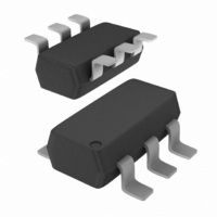
... Pb−Free Package (Note: Microdot may be in either location) ORDERING INFORMATION Device Package Shipping NSS20201MR6T1G TSOP−6 3000/Tape & Reel (Pb−Free) †For information on tape and reel specifications, including part orientation and tape sizes, please refer to our Tape and Reel Packaging Specifications Brochure, BRD8011/D ...

Page 2

... Base −Emitter Turn−on Voltage (Note 1 2 Cutoff Frequency (I = 100 mA 5 100 MHz C CE Output Capacitance (f = 1.0 MHz) 3. Pulsed Condition: Pulse Width ≤ 300 msec, Duty Cycle ≤ 2%. NSS20201MR6T1G (T = 25°C unless otherwise noted http://onsemi.com 2 Symbol Min Typ Max (BR)CEO 20 − ...

Page 3

... Pb−Free strategy and soldering details, please download the ON Semiconductor Soldering and Mounting Techniques Reference Manual, SOLDERRM/D. NSS20201MR6T1G TSOP−6 CASE 318G−02 ISSUE N NOTES: 1. DIMENSIONING AND TOLERANCING PER ANSI Y14.5M, 1982. 2. CONTROLLING DIMENSION: MILLIMETER. ...

Page 4

... P.O. Box 61312, Phoenix, Arizona 85082−1312 USA Phone: 480−829−7710 or 800−344−3860 Toll Free USA/Canada Fax: 480−829−7709 or 800−344−3867 Toll Free USA/Canada Email: orderlit@onsemi.com NSS20201MR6T1G N. American Technical Support: 800−282−9855 Toll Free USA/Canada Japan: ON Semiconductor, Japan Customer Focus Center 2− ...

Related keywords