BUL7216 STMicroelectronics, BUL7216 Datasheet
BUL7216
Specifications of BUL7216
Available stocks


Related parts for BUL7216


BUL7216 Summary of contents
Page 1
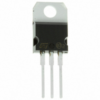
... Order code Marking BUL7216 BUL7216 BULB7216-1 BULB7216 BULB7216T4 BULB7216 November 2007 High voltage fast-switching NPN power transistor TO-220 D Figure 1. Internal schematic diagram Package TO-220 2 I PAK 2 D PAK Rev 2 BULB7216 BUL7216 PAK PAK Packaging Tube Tube Tape and reel 1/13 www.st.com 13 ...
Page 2
... Contents Contents 1 Electrical ratings . . . . . . . . . . . . . . . . . . . . . . . . . . . . . . . . . . . . . . . . . . . . 3 2 Electrical characteristics . . . . . . . . . . . . . . . . . . . . . . . . . . . . . . . . . . . . . 4 2.1 Electrical characteristics (curves Test circuit . . . . . . . . . . . . . . . . . . . . . . . . . . . . . . . . . . . . . . . . . . . . . . . . . 7 4 Package mechanical data . . . . . . . . . . . . . . . . . . . . . . . . . . . . . . . . . . . . . 8 5 Revision history . . . . . . . . . . . . . . . . . . . . . . . . . . . . . . . . . . . . . . . . . . . 12 2/13 BULB7216 - BUL7216 ...
Page 3
... BULB7216 - BUL7216 Electrical ratings 1 Table 2. Absolute maximum rating Symbol V Collector-emitter voltage (V CES V Collector-emitter voltage (I CEO V Emitter-base voltage (I EBO I Collector current C I Collector peak current ( Base current B I Base peak current ( Total dissipation at T tot T Storage temperature stg T Max. operating junction temperature J Table 3 ...
Page 4
... Pulsed duration = 300 µs, duty cycle ≤ 1.5% 4/13 Parameter Test conditions V =1600 =1600 =680 =1600 =1600 = P.W.= 300 µ BE(off) BULB7216 - BUL7216 Min. Typ 125 ° 125 °C C 700 12 1600 100 100 400 125 -0 D.C 1 Max. Unit 0.1 mA 0 0.1 0 1.5 V ...
Page 5
... BULB7216 - BUL7216 2.1 Electrical characteristics (curves) Figure 2. Derating curve Figure 4. DC current gain Figure 6. Collector - emitter saturation voltage Electrical characteristics Figure 3. Reverse biased safe operating area Figure 5. DC current gain Figure 7. Base - emitter saturation voltage 5/13 ...
Page 6
... Electrical characteristics Figure 8. Resistive load switching time Figure 9. 6/13 BULB7216 - BUL7216 Resistive load switching time ...
Page 7
... BULB7216 - BUL7216 3 Test circuit Figure 10. Energy rating test circuit Figure 11. Resistive load switching test circuit 1) Fast electronic switch 2) Non-inductive resistor Test circuit 7/13 ...
Page 8
... These packages have a Lead-free second level interconnect. The category of second level interconnect is marked on the package and on the inner box label, in compliance with JEDEC Standard JESD97. The maximum ratings related to soldering conditions are also marked on the inner box label. ECOPACK trademark. ECOPACK specifications are available at: 8/13 BULB7216 - BUL7216 www.st.com ...
Page 9
... BULB7216 - BUL7216 Dim L20 L30 ∅P Q TO-220 mechanical data mm Min Typ Max 4.40 4.60 0.61 0.88 1.14 1.70 0.49 0.70 15.25 15.75 1.27 10 10.40 2.40 2.70 4.95 5.15 1.23 1.32 6.20 6.60 2.40 2. 3.50 3.93 16.40 28.90 3.75 3.85 2.65 2.95 ...
Page 10
... BULB7216 - BUL7216 inch MIN. TYP. MAX. 0.173 0.181 0.094 0.107 0.024 0.034 0.044 0.066 0.019 0.027 0.048 0.052 0.352 0.368 0.094 0.106 0.194 ...
Page 11
... BULB7216 - BUL7216 DIM Weight : 1.38 g (typ.) - The planaty of the slug must be within 30 µm 2 TO-263 (D PAK) MECHANICAL DATA mm MIN. TYP. MAX. 4.40 4.60 2.49 2.69 0.03 0.23 0.70 0.93 1.14 1.70 0.45 0.60 1.23 1.36 8.95 9.35 8.00 10.00 10.40 8.50 4.88 5 ...
Page 12
... Revision history 5 Revision history Table 5. Document revision history Date 17-Jan-2006 28-Nov-2007 12/13 Revision 1 First release Added packages D PAK and I BULB7216 - BUL7216 Changes 2 PAK ...
Page 13
... BULB7216 - BUL7216 Information in this document is provided solely in connection with ST products. STMicroelectronics NV and its subsidiaries (“ST”) reserve the right to make changes, corrections, modifications or improvements, to this document, and the products and services described herein at any time, without notice. All ST products are sold pursuant to ST’s terms and conditions of sale. ...