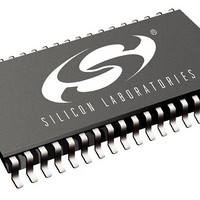
SI3210M-KTR Silicon Laboratories Inc, SI3210M-KTR Datasheet - Page 138

SI3210M-KTR
Manufacturer Part Number
SI3210M-KTR
Description
RF Wireless Misc Sgl Ch SLIC/Codec w/ MOSFET Decoder
Manufacturer
Silicon Laboratories Inc
Type
ProSLIC Programmable CMOS SLICr
Datasheet
1.SI3210MPPQX-EVB.pdf
(146 pages)
Specifications of SI3210M-KTR
Operating Frequency
200 MHz
Supply Current
4 mA
Operating Temperature Range
- 40 C to + 100 C
Package / Case
TSSOP-14
Mounting Style
SMD/SMT
Lead Free Status / RoHS Status
Lead free / RoHS Compliant
- Current page: 138 of 146
- Download datasheet (860Kb)
Si3210/Si3211
8.3.2. PCB Land Pattern: 16-Pin ESOIC
Figure 38 illustrates the recommended land pattern for the Si3201 SOIC-16 package. Table 53 lists the values for
the dimensions shown in the illustration.
138
Y2
Notes:
General
Solder Mask Design
Stencil Design
Card Assembly
Dimension
1. All dimensions shown are in millimeters (mm) unless otherwise noted.
2. Dimensioning and Tolerancing per ASME Y14.5M-1994.
3. This Land Pattern Design is based on IPC-7351 pattern SOIC127P600X175-17N.
1. All metal pads are to be non-solder mask defined (NSMD). Clearance between the solder
1. A stainless steel, laser-cut and electro-polished stencil with trapezoidal walls should be used
2. The stencil thickness should be 0.125mm (5 mils).
3. The ratio of stencil aperture to land pad size should be 1:1 for all perimeter pads.
1. A No-Clean, Type-3 solder paste is recommended.
2. The recommended card reflow profile is per the JEDEC/IPC J-STD-020C specification for
C1
X1
Y1
X2
mask and the metal pad is to be 60m minimum, all the way around the pad.
to assure good solder paste release.
Small Body Components.
E
Table 53. SOIC-16 PCB Land Pattern Dimensions
Figure 38. SOIC-16 PCB Land Pattern Drawing
Pin pad column spacing
Thermal pad length
Thermal pad width
Pin pad row pitch
Pin pad length
Pin pad width
Feature
Rev. 1.5
5.30
0.50
1.45
2.20
3.50
Min
1.27 BSC
Max
5.40
2.30
3.60
0.60
1.55
Related parts for SI3210M-KTR
Image
Part Number
Description
Manufacturer
Datasheet
Request
R

Part Number:
Description:
IC SLIC/CODEC PROG 1CH 38QFN
Manufacturer:
Silicon Laboratories Inc
Datasheet:
Part Number:
Description:
IC SLIC/CODEC PROG 1CH 38TSSOP
Manufacturer:
Silicon Laboratories Inc
Datasheet:

Part Number:
Description:
IC SLIC/CODEC PROG 1CH 38QFN
Manufacturer:
Silicon Laboratories Inc
Datasheet:
Part Number:
Description:
IC SLIC/CODEC PROG 1CH 38TSSOP
Manufacturer:
Silicon Laboratories Inc
Datasheet:
Part Number:
Description:
IC SLIC/CODEC PROG 1CH 38TSSOP
Manufacturer:
Silicon Laboratories Inc
Datasheet:
Part Number:
Description:
IC SLIC/CODEC PROG 38TSSOP
Manufacturer:
Silicon Laboratories Inc
Datasheet:
Part Number:
Description:
Manufacturer:
Silicon Laboratories Inc
Datasheet:
Part Number:
Description:
Manufacturer:
Silicon Laboratories Inc
Datasheet:
Part Number:
Description:
Manufacturer:
Silicon Laboratories Inc
Datasheet:

Part Number:
Description:
RF Wireless Misc Sgl Ch SLIC/Codec w/ MOSFET Decoder
Manufacturer:
Silicon Laboratories Inc
Datasheet:
Part Number:
Description:
C�/SI3210 QFN EVALUATION BOARD WITH DISCRETE LINE INTERFACE
Manufacturer:
Silicon Laboratories Inc
Datasheet:
Part Number:
Description:
QFN 38/I�/SINGLE-CHANNEL SLIC/CODEC WITH DTMF DECODER AND BJT/INDUCTOR DC-D
Manufacturer:
Silicon Laboratories Inc
Part Number:
Description:
IC SLIC/CODEC PROGRAMMBL 38TSSOP
Manufacturer:
Silicon Laboratories Inc
Datasheet:
Part Number:
Description:
IC SLIC/CODEC PROG 38TSSOP
Manufacturer:
Silicon Laboratories Inc
Datasheet:

Part Number:
Description:
IC SLIC/CODEC PROG 38QFN
Manufacturer:
Silicon Laboratories Inc
Datasheet:


