STB5610 STMicroelectronics, STB5610 Datasheet
STB5610
Specifications of STB5610
Available stocks


Related parts for STB5610


STB5610 Summary of contents
Page 1
... Active antenna sensor ■ Smart chip enable function for power consumption optimization ■ ESD protected Description The STB5610, using ST RF bipolar technology, implements a global positioning system (GPS) RF front-end. Table 1. Device summary Order code STB5610ETR February 2009 This is information on a product still in production but not recommended for new designs. ...
Page 2
... Input control pins table (the logic levels are TTL compatible 3.5 Output control pins table . . . . . . . . . . . . . . . . . . . . . . . . . . . . . . . . . . . . . . 9 4 Application information . . . . . . . . . . . . . . . . . . . . . . . . . . . . . . . . . . . . . 10 5 Package information . . . . . . . . . . . . . . . . . . . . . . . . . . . . . . . . . . . . . . . . 13 6 Revision history . . . . . . . . . . . . . . . . . . . . . . . . . . . . . . . . . . . . . . . . . . . 14 2/15 LNA section . . . . . . . . . . . . . . . . . . . . . . . . . . . . . . . . . . . . . . . . . . . . . . . 3 RF amplifier plus mixer section . . . . . . . . . . . . . . . . . . . . . . . . . . . . . . . . 3 IF section . . . . . . . . . . . . . . . . . . . . . . . . . . . . . . . . . . . . . . . . . . . . . . . . . 3 Output section . . . . . . . . . . . . . . . . . . . . . . . . . . . . . . . . . . . . . . . . . . . . . 3 Power supplies . . . . . . . . . . . . . . . . . . . . . . . . . . . . . . . . . . . . . . . . . . . . . 4 VCO and PLL . . . . . . . . . . . . . . . . . . . . . . . . . . . . . . . . . . . . . . . . . . . . . . 4 Antenna sensor circuitry . . . . . . . . . . . . . . . . . . . . . . . . . . . . . . . . . . . . . 4 Chip enable . . . . . . . . . . . . . . . . . . . . . . . . . . . . . . . . . . . . . . . . . . . . . . . 4 STB5610 ...
Page 3
... STB5610 1 Block diagram and functional description 1.1 Block diagram Figure 1. Block diagram Passive Antenna Two gain LNA Gain Select. 16.368 MHz Quartz 1.2 Functional description 1.2.1 LNA section The RF input signal is amplified by two gain levels LNA. Using gain control pin the LNA gain is set support passive antenna support active antenna ...
Page 4
... Block diagram and functional description 1.2.5 Power supplies The STB5610, has been designed to support from 2 3.6 V supply voltage. 1.2.6 VCO and PLL Using external tank the VCO is able to provide very low phase noise signal. Through the frequency selector pin the VCO signal is set at 1554.96 MHz and at 1571.328 MHz. The on- chip reference oscillator uses a low cost 16 ...
Page 5
... STB5610 2 Pin description Figure 2. Pin connection (top view) Table 2. Pin description Pin # Vcc_XTAL 1 Vcc_Logic Vcc_VCO 4 GND 5 TNK1 6 TNK2 7 GND 8 GND 9 IF1+ 10 IF1- 11 GND Pin name Vcc_XTAL Power supply Vcc_Logic Power supply LF Loop filter Vcc_VCO Power supply GND Ground TNK1 Tank Input ...
Page 6
... GND Ground Vcc_Logic2 Supply Voltage CE2 Chip Enable (no data) CE Chip Enable Fselect Frequency Selector GND_IF Ground IF2- Lim. Amp. Output IF2+ Lim. Amp. Output GND_IF Ground Vcc_IF Supply Voltage GND_XTAL Ground XTAL_in Crystal Input XTAL_out Crystal Output GND_XTAL Ground STB5610 Description ...
Page 7
... STB5610 3 Electrical specification 3.1 Absolute maximum ratings Table 3. Absolute maximum ratings Symbol V Supply voltage CC T Junction operating temperature j 3.2 Thermal data Table 4. Thermal data Symbol R Thermal resistance junction to case thj-case 3.3 Electrical characteristics Table 5. Electrical characteristics ( ± Symbol Parameter Supply V Supply voltage ...
Page 8
... GC Pin (LNA gain control pin) Table 7. CE2 Pin (analog portion enable pin) 8/ °C) case Test conditions kHz, SSB (10 kHz PLL closed loop bandwidth) Logic level Low High Logic level Low High STB5610 Min. Typ. Max. 1.4 1.575 30 60 2.4 30 -60 Vcc-0.4 Vcc 0 0+0.4 16 ...
Page 9
... The Asout pin output provides information on Antenna current consumption. Table 10. ASout pin (antenna sensor pin referred to external sensing resistor of 10 Ohm. Application requiring higher or lower current threshold should adjust the resistor value appropiately. 2. The logic levels are referred to STB5610 supply voltage. Logic level Low High Logic level ...
Page 10
... Application information 4 Application information Figure 3. Application board schematic (active antenna) 10/ FSELEC GND_I IF2- IF2 + 4 2 GND GND XTA GND STB5610 NAO ccRF D_R ND_ ...
Page 11
... STB5610 Figure 4. Application board layout (active antenna) Table 11. Bill of materials Q.ty Reference designator R3 R4,R7,R8,R9 2 R10,R11 2 C1, C7, C8 C10 1 C11 1 C12 4 C16,C19 Value 470 ohm 6.2 kohm 1 kohm 10 ohm 10 kohm 100 ohm 56 pF Murata (series GRM18 Murata (series GRM18) 1 µF (electrolytic) Kemet (series T491) Case A 2 ...
Page 12
... STB5610 L4931ABD33 8+8 pin connector SMA connector (female) NSVA352 (1) DFC21R57P002HHA SMV1405-079 SMV1405-079 DHF32UM-1SJ(16.368 MHz) STB5610 Manufacturer Murata (series GRM18) Murata (series GRM18) Murata (series GRM18) Murata (series GRM18) Coilcraft (series 1008CS) Murata (series LQP18M) Coilcraft (series 1008CS) Murata (series LQP18M) Murata (series LQW18) ...
Page 13
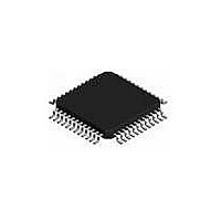
... STB5610 5 Package information In order to meet environmental requirements, ST offers these devices in different grades of ® ECOPACK packages, depending on their level of environmental compliance. ECOPACK specifications, grade definitions and product status are available at: www.st.com. ® ECOPACK trademark. Figure 5. LQFP48 mechanical data and package dimensions DIM. ...
Page 14
... Revision history 6 Revision history Table 12. Document revision history Date 20-Dec2003 12-Feb-2009 14/15 Revision 3 Initial release. Document reformatted. 4 Document status changed from datasheet to not for new design. Updated Section 5: Package information on page STB5610 Changes 13. ...
Page 15
... STB5610 Information in this document is provided solely in connection with ST products. STMicroelectronics NV and its subsidiaries (“ST”) reserve the right to make changes, corrections, modifications or improvements, to this document, and the products and services described herein at any time, without notice. All ST products are sold pursuant to ST’s terms and conditions of sale. ...