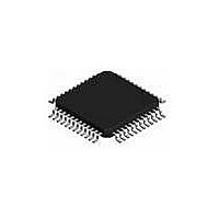
STB5610TR STMicroelectronics, STB5610TR Datasheet

STB5610TR
Specifications of STB5610TR
Related parts for STB5610TR
STB5610TR Summary of contents
Page 1
Features ■ One chip system to interface GPS antenna to GPS microcontroller ■ Able to support active and passive antenna ■ Minimum external components ■ Compatible with GPS L1 SPS signal and Galileo frequencies ■ CMOS output levels ■ 2.7 ...
Page 2
Contents Contents 1 Block diagram and functional description . . . . . . . . . . . . . . . . . . . . . . . 3 1.1 Block diagram . . . . . ...
Page 3
STB5610 1 Block diagram and functional description 1.1 Block diagram Figure 1. Block diagram Passive Antenna Two gain LNA Gain Select. 16.368 MHz Quartz 1.2 Functional description 1.2.1 LNA section The RF input signal is amplified by two gain levels ...
Page 4
Block diagram and functional description 1.2.5 Power supplies The STB5610, has been designed to support from 2 3.6 V supply voltage. 1.2.6 VCO and PLL Using external tank the VCO is able to provide very low phase noise ...
Page 5
STB5610 2 Pin description Figure 2. Pin connection (top view) Table 2. Pin description Pin # ...
Page 6
Pin description Table 2. Pin description (continued) Pin # ...
Page 7
STB5610 3 Electrical specification 3.1 Absolute maximum ratings Table 3. Absolute maximum ratings Symbol V Supply voltage CC T Junction operating temperature j 3.2 Thermal data Table 4. Thermal data Symbol R Thermal resistance junction to case thj-case 3.3 Electrical ...
Page 8
Electrical specification Table 5. Electrical characteristics (continued ± Symbol Parameter Differential output Z OUT impedance f Input signal RF RF Voltage convertion G gain First limiting amplifier G Voltage gain Differential output Z OUT ...
Page 9
STB5610 Table 8. CE pin (total chip enable pin) Table 9. FSELECT (frequencies Selector Pin) 3.5 Output control pins table The Asout pin output provides information on Antenna current consumption. Table 10. ASout pin (antenna sensor pin ...
Page 10
Application information 4 Application information Figure 3. Application board schematic (active antenna) 10/ FSELEC GND_I IF2- IF2 + 4 2 GND _ ...
Page 11
STB5610 Figure 4. Application board layout (active antenna) Table 11. Bill of materials Q.ty Reference designator R3 R4,R7,R8,R9 2 R10,R11 2 C1, C7, C8 C10 1 ...
Page 12
Application information Table 11. Bill of materials (continued) Q.ty Reference designator 7 C3,C5, C6,C13,C14,C21,C23 3 C18, C20,C26 5 C15,C17,C22,C25,C27 1 C28 U2, U3 ...
Page 13
STB5610 5 Package information In order to meet environmental requirements, ST offers these devices in different grades of ® ECOPACK packages, depending on their level of environmental compliance. ECOPACK specifications, grade definitions and product status are available at: www.st.com. ® ...
Page 14
Revision history 6 Revision history Table 12. Document revision history Date 20-Dec2003 12-Feb-2009 14/15 Revision 3 Initial release. Document reformatted. 4 Document status changed from datasheet to not for new design. Updated Section 5: Package information on page STB5610 Changes ...
Page 15
... STB5610 Information in this document is provided solely in connection with ST products. STMicroelectronics NV and its subsidiaries (“ST”) reserve the right to make changes, corrections, modifications or improvements, to this document, and the products and services described herein at any time, without notice. All ST products are sold pursuant to ST’s terms and conditions of sale. ...


