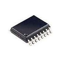
74HCT9046APW NXP Semiconductors, 74HCT9046APW Datasheet - Page 20

74HCT9046APW
Manufacturer Part Number
74HCT9046APW
Description
Phase Locked Loops (PLL) PLL BAND GAP CNTRL W/VCO
Manufacturer
NXP Semiconductors
Type
PLLr
Datasheet
1.74HCT9046AN112.pdf
(43 pages)
Specifications of 74HCT9046APW
Number Of Circuits
1
Supply Voltage (max)
5.5 V
Supply Voltage (min)
4.5 V
Maximum Operating Temperature
+ 125 C
Minimum Operating Temperature
- 40 C
Mounting Style
SMD/SMT
Operating Supply Voltage
4.5 V to 5.5 V
Package / Case
TSSOP-16
Lead Free Status / RoHS Status
Lead free / RoHS Compliant
Other names
74HCT9046APW,112
Available stocks
Company
Part Number
Manufacturer
Quantity
Price
Company:
Part Number:
74HCT9046APW
Manufacturer:
NXP
Quantity:
12 500
Company:
Part Number:
74HCT9046APW,118
Manufacturer:
CY
Quantity:
490
NXP Semiconductors
12. Dynamic characteristics
Table 6.
GND = 0 V; t
74HCT9046A_6
Product data sheet
Symbol
T
Phase comparator section
t
t
t
t
V
VCO section
f
General
C
T
Phase comparator section
t
t
t
t
VCO section
pd
en
dis
t
0
pd
en
dis
t
amb
f
f/f
amb
i(p-p)
PD
= 25 C
= 40 C to +85 C
Dynamic characteristics
r
= t
Parameter
propagation delay
enable time
disable time
transition time
peak-to-peak input voltage
frequency deviation
center frequency
relative frequency variation
duty cycle
power dissipation capacitance
propagation delay
enable time
disable time
transition time
f
= 6 ns; C
L
= 50 pF.
[1]
Rev. 06 — 15 September 2009
Conditions
SIG_IN, COMP_IN to PC1_OUT;
V
SIG_IN, COMP_IN to PCP_OUT;
V
SIG_IN, COMP_IN to PC2_OUT;
V
SIG_IN, COMP_IN to PC2_OUT;
V
V
pin SIGN_IN or COMP_IN;
V
V
R1 = 10 k ; R2 = 10 k ; C1 = 1 nF
V
V
R2 =
and
V
V
R2 =
and
V
C1 = 100 pF; see
VCO_OUT; V
SIG_IN, COMP_IN to PC1_OUT;
V
SIG_IN, COMP_IN to PCP_OUT;
V
SIG_IN, COMP_IN to PC2_OUT;
V
SIG_IN, COMP_IN to PC2_OUT;
V
V
CC
CC
CC
CC
CC
CC
CC
CC
VCO_IN
CC
VCO_IN
CC
CC
CC
CC
CC
CC
= 4.5 V; see
= 4.5 V; see
31
31
= 4.5 V; see
= 4.5 V; see
= 4.5 V; see
= 4.5 V; AC coupled; f
= 5.0 V; V
= 4.5 V; duty cycle = 50 %;
= 5 V; duty cycle = 50 %;
= 4.5 V; R1 = 100 k ; R2 =
= 4.5 V; see
= 4.5 V; see
= 4.5 V; see
= 4.5 V; see
= 4.5 V; see
= 0.5V
= 0.5V
; C1 = 40 pF; see
; C1 = 40 pF; see
CC
VCO_IN
CC
CC
= 4.5 V
Figure 19
Figure 19
Figure 18
Figure 18
Figure 18
Figure 18
Figure 18
Figure 19
Figure 19
Figure 18
; R1 = 4.3 k ;
; R1 = 3 k ;
Figure 24
= 3.9 V;
i
= 1 MHz
Figure 23
Figure 23
and
25
PLL with band gap controlled VCO
;
[2][3]
[4]
[5]
[6]
74HCT9046A
Min
-
-
-
-
-
-
11.0
-
-
-
-
-
-
-
-
-
10
Typ
23
35
30
36
7
50
-
15.0
16.0
0.4
50
20
-
-
-
-
-
© NXP B.V. 2009. All rights reserved.
Max
40
68
56
65
15
-
+10
-
-
-
-
-
50
85
70
81
19
20 of 43
Unit
ns
ns
ns
ns
ns
mV
%
MHz
MHz
%
%
pF
ns
ns
ns
ns
ns


