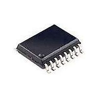
74HCT9046AD NXP Semiconductors, 74HCT9046AD Datasheet - Page 13

74HCT9046AD
Manufacturer Part Number
74HCT9046AD
Description
Phase Locked Loops (PLL) PHASE LOCKED LOOP W/VCO
Manufacturer
NXP Semiconductors
Type
PLLr
Datasheet
1.74HCT9046AN112.pdf
(43 pages)
Specifications of 74HCT9046AD
Number Of Circuits
1
Supply Voltage (max)
5.5 V
Supply Voltage (min)
4.5 V
Maximum Operating Temperature
+ 125 C
Minimum Operating Temperature
- 40 C
Mounting Style
SMD/SMT
Operating Supply Voltage
5 V
Package / Case
SOIC-16
Lead Free Status / RoHS Status
Lead free / RoHS Compliant
Other names
74HCT9046AD,112
Available stocks
Company
Part Number
Manufacturer
Quantity
Price
Company:
Part Number:
74HCT9046AD
Manufacturer:
INTEL
Quantity:
3
Company:
Part Number:
74HCT9046AD
Manufacturer:
PHILIPS
Quantity:
1 893
Part Number:
74HCT9046AD
Manufacturer:
NXP/恩智浦
Quantity:
20 000
NXP Semiconductors
74HCT9046A_6
Product data sheet
Fig 12. Simple loop filter for PC2 without damping
R bias
I
17
cp
a. Simple loop filter for PC2
without damping
1
=
INPUT
R
----------- -
17
8.4 Loop filter component selection
bias
C2
C2
Using this equivalent resistance R3' for the filter design the voltage can now be expressed
as a transfer function of PC2; assuming ripple (f
Again this illustrates the supply voltage independent behavior of PC2.
Examples of PC2 combined with a passive filter are shown in
shows that PC2 with only a C2 filter behaves as a high-gain filter. For stability the damped
version of
Practical design values for R
to 15 k for the filter design. Higher values for R3' require lower values for the filter
capacitance which is very advantageous at low values of the loop natural frequency
K
I
cp
PC2
=
001aak449
OUTPUT
R3' C2
=
----- - V r
4
5
Figure 13
F
A
(j )
with series resistance R4 is preferred.
Rev. 06 — 15 September 2009
b. Amplitude characteristic
F
1/ A
j
bias
1
=
are between 25 k and 250 k with R3' = 1.5 k
---------------------------- -
1 A
+
1
j
001aak450
1
----------- -
j
r
1
= f
1
PLL with band gap controlled VCO
i
) is suppressed, as:
c. Pole zero diagram
Figure 12
A = DC gain limit, due to leakage
74HCT9046A
© NXP B.V. 2009. All rights reserved.
and 13.
001aak451
1/ A
1
Figure 12
13 of 43
n
.


