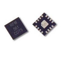
TXC100 RFM, TXC100 Datasheet - Page 4

TXC100
Manufacturer Part Number
TXC100
Description
RF Transceiver Transmitter 300-450MHz ASK/FSK
Manufacturer
RFM
Datasheet
1.TXC100.pdf
(11 pages)
Specifications of TXC100
Output Power
- 10 dBm to + 10 dBm
Operating Supply Voltage
2.5 V, 3.3 V
Mounting Style
SMD/SMT
Package / Case
TQFN-16
Minimum Operating Temperature
- 40 C
Lead Free Status / RoHS Status
Lead free / RoHS Compliant
www.RFM.com
©RF Monolithics, Inc.
5
6
7
8
10, 9
13, 12, 11
14
15
16
Clk
V
ES
PA
Clk[1..0]
FreqDev[2..0]
Xtal1
Xtal2/REF
GND
Email:
DDPA
Out
Out
Out
info@rfm.com
IN
The clock output is a scaled and buffered version of the crystal frequency, which may be used to drive external logic or a microprocessor.
The frequency is programmable through Pins 9 (Clk0) and 10(Clk1) as below:
fc = Crystal Frequency
This pin is a power supply voltage source for the transmitter power amplifier. Bypass this pin as close as possible with a 0.01 µF and 220
pF capacitor. ES
This pin can be used to supply voltage to the power amplifier instead of V
to be adjusted in ASK mode. Reducing the rise and fall times reduces the spectral bandwidth of the modulated output signal, and also
reduces average transmitter power. Rise and fall times are adjusted by placing a resistor in the range of 1K to 5K in series with this
output, as close as possible to the TXC100 IC to minimize circuit parasitics. The power amplifier side of the resistor should be bypassed
with 680 pF and 220 pF capacitors in parallel, as close to the resistor as possible.
Power Amplifier - the power amplifier is an open-drain, Class C amplifier designed for a load impedance at PA
ohms. The power amplifier requires a DC path to the supply voltage through a series inductor, which can be part of the output matching
network. A 50 ohm antenna matching network is shown in the Typical Application Circuit section. The matching network also suppresses
carrier harmonics to aid in compliance testing.
See description for Pin 5
The Frequency Deviation Pins set the amount of deviation between data logic states in FSK mode. Frequency deviation is programmable
through pins 11, 12, 13 as shown in the table below:
Deviation values are approximate and apply to a properly loaded crystal. Crystal characteristics and loading behavior can vary between
suppliers.
External Crystal Input 1 presents a capacitance of 3 pF to GND in ASK and FSK (Data
package capacitance, presenting a total load of about 4.5 pF.
External Crystal Input 2 presents a capacitance of 3 pF to GND in ASK and FSK(Data
package capacitance, presenting a total load of about 4.5 pF.
The External Ref Input allows an external frequency source to be used to obtain the desired transmit frequency. In this case, the Xtal1
input must be bypassed with a 0.01µF capacitor, and a 0.01µF series capacitance should be added into External Reference input.
Crystal Reference - the Xtal1 and Xtal2 inputs are designed to present a 3 pF load to GND to each reference crystal connection.
Including PCB parasitic capacitances, this increases to about 4.5 pFat each connection. In ASK mode, the full 3 pF load is applied to the
crystal allowing it to oscillate at the desired frequency. In FSK mode, a portion of the 3 pF load is removed in response to a logic high
being applied to the Data
use a crystal with large motional capacitance or reduce PCB parasitic capacitance to the extent possible.
Connect to system ground.
Note: The ground pad in the middle of the package is the power amplifier ground. It must be connected to system ground thru a low
inductance path.
.125 x Max
.250 x Max
.375 x Max
.500 x Max
.625 x Max
.750 x Max
.875 x Max
DEV ∆ ∆ ∆ ∆
Max
Clk0
0
1
0
1
Out
is the alternate power amplifier voltage source as discussed below.
DEV 2
Clk1
0
0
0
0
1
1
1
1
0
0
1
1
IN
(pin 2) as set by the frequency deviation pins DEV[0..2] (11,12,13). To achieve larger frequency deviations,
DEV 1
Clk
fc/16
fc/4
fc/8
0
0
1
1
0
0
1
1
0
Out
DEV 0
0
1
0
1
0
1
0
1
DDPA
, allowing the on/off rise and fall times of the power amplifier
IN
IN
logic low) mode. Circuit parasitics add to this
logic low) modes. Circuit parasitics add to this
OUT
(pin 8) of about 250
TXC100 - 08/18/10
Page 4 of 11


