BGM 781N11 E6327 Infineon Technologies, BGM 781N11 E6327 Datasheet
BGM 781N11 E6327
Specifications of BGM 781N11 E6327


Related parts for BGM 781N11 E6327

BGM 781N11 E6327 Summary of contents
Page 1
& ...
Page 2
... Infineon Technologies Office. Infineon Technologies Components may only be used in life-support devices or systems with the express written approval of Infineon Technologies failure of such components can reasonably be expected to cause the failure of that life-support device or system affect the safety or effectiveness of that device or system. Life support devices or systems are intended to be implanted in the human body support and/or maintain and sustain and/or protect human life ...
Page 3
Oct. 2010 Revision History: GPS Front-End Module, Rev.3.2 Previous Version: 2009-10-30, Rev.3.1 Page Subjects (major changes since last revision) 10 Package pin tolerances changed from 35µm to 50µm Data Sheet 3 BGM781N11 Rev.3.2, 2010-10-28 ...
Page 4
GPS Front-End Module 1 GPS Front-End Module Features • Operating frequency: 1575.42 MHz • High Gain: 18.6 dB • Low Noise Figure: 1.7 dB • Low current consumption: 3.3 mA • Out-of-band rejection in cellular bands: 80 dBc • Input ...
Page 5
Description The BGM781N11 is a combination of a low-insertion-loss pre-filter with Infineon’s high performance low noise amplifier (LNA) and a high-attenuation post-filter for Global Positioning System (GPS) applications. Through the low insertion loss of the filters, the BGM781N11 provides ...
Page 6
Table 2 Maximum Ratings (cont’d) 1) Parameter RF input power out of band Total power dissipation Junction temperature Ambient temperature range Storage temperature range ESD capability HBM of all pins, with pin 6 and GND middle island pin 11 tied ...
Page 7
Electrical Characteristics Table 3 Electrical Characteristics: Parameter Supply Voltage Supply Current Power On Control Voltage Power On Control Current 2) Power Gain Settling Time Passband Parameters @ f = 1575.42 MHz Insertion Power Gain 3) Noise Figure Input Return ...
Page 8
Application Information 4.1 Application Circuit PON VCC C1 RFIN Figure 2 Application circuit with external components Table 4 Bill of Materials Name Value 1 μ 3 BGM781N11 Data Sheet BGM781N11 (Topview) BG2 ...
Page 9
Application Board Figure 3 Top view of application board Figure 4 Cross section view of application board Data Sheet BGM781_AppBoard_Layout_top.vsd BGM781_AppBoard_Cross_Section.vsd 9 BGM781N11 Application Information Copper, 35μm, gold plated Rogers RO4003C, 0.2mm Copper, 35μm FR4, 0.8mm Copper, 35μm Rev.3.2, ...
Page 10
Package Information Figure 5 Side and bottom views of TSNP-11-2 package Figure 6 Marking layout Data Sheet Pin 1 marking Laser marking BGM781N11 M781 Type code 2010 1025 Date code (YYWW) TSNP11_Marking_Layout_BGM781.vsd 10 BGM781N11 Package Information Rev.3.2, ...
Page 11
Figure 7 Recommended TSNP-11-2 footprint for optimum RF performance Figure 8 Alternative TSNP-11-2 footprint for low cost PCB designs Data Sheet 11 BGM781N11 Package Information Rev.3.2, 2010-10-28 ...
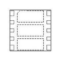
Page 12
Packing Information Figure 9 TSNP-11-2 carrier tape Figure 10 TSNP-11-2 pin 1 orientation in tape Data Sheet 12 BGM781N11 Packing Information Rev.3.2, 2010-10-28 ...