MJH11022G ON Semiconductor, MJH11022G Datasheet - Page 3
MJH11022G
Manufacturer Part Number
MJH11022G
Description
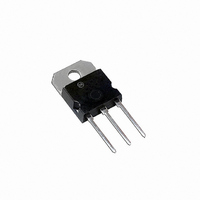
TRANS DARL NPN 15A 250V TO218
Manufacturer
ON Semiconductor
Type
Power, Switchr
Specifications of MJH11022G
Transistor Type
NPN - Darlington
Current - Collector (ic) (max)
15A
Voltage - Collector Emitter Breakdown (max)
250V
Vce Saturation (max) @ Ib, Ic
4V @ 150mA, 15A
Current - Collector Cutoff (max)
1mA
Dc Current Gain (hfe) (min) @ Ic, Vce
400 @ 10A, 5V
Power - Max
150W
Frequency - Transition
3MHz
Mounting Type
Through Hole
Package / Case
SOT-93, TO-218 (Straight Leads)
Configuration
Single
Transistor Polarity
NPN
Mounting Style
SMD/SMT
Collector- Emitter Voltage Vceo Max
250 V
Emitter- Base Voltage Vebo
5 V
Collector- Base Voltage Vcbo
250 V
Maximum Dc Collector Current
15 A
Power Dissipation
150 W
Maximum Operating Temperature
+ 150 C
Continuous Collector Current
15 A
Dc Collector/base Gain Hfe Min
100, 400
Minimum Operating Temperature
- 65 C
Current, Gain
100
Current, Input
0.5 A
Current, Output
15 A
Package Type
SOT-93 (TO-218)
Polarity
NPN
Primary Type
Si
Voltage, Collector To Emitter, Saturation
4 V
Voltage, Input
5 V
Voltage, Output
250 V
Lead Free Status / RoHS Status
Lead free / RoHS Compliant
Other names
MJH11022GOS
Available stocks
Company
Part Number
Manufacturer
Quantity
Price
Company:

Part Number:
MJH11022G
Manufacturer:
ON
Quantity:
30 000
Company:
Part Number:
MJH11022G
Manufacturer:
MOTOROLA
Quantity:
10 000
Part Number:
MJH11022G
Manufacturer:
ON/安森美
Quantity:
20 000


5.0
2.0
1.0
0.5
0.2
30
20
10
0.07
0.05
0.03
0.02
0.01
0
R
D
1.0
0.7
0.5
0.3
0.2
0.1
B
1
0.01
1N5825 used above I
MSD6100 used below I
, must be fast recovery types, e.g.:
& R
T
C
Figure 4. Maximum Rated Forward Bias
D = 0.5
0.2
0.1
0.05
0.02
SINGLE PULSE
C
= 25°C SINGLE PULSE
varied to obtain desired current levels
0.02
V
WIRE BOND LIMIT
THERMAL LIMIT
SECOND BREAKDOWN LIMIT
CE
Safe Operating Area (FBSOA)
, COLLECTOR-EMITTER VOLTAGE (VOLTS)
0.03
2.0
3.0
0.05
0.01
B
5.0
0.5 ms
≈ 100 mA
B
1.0 ms
≈ 100 mA
0.1
MJH11017, MJH11018
MJH11019, MJH11020
MJH11021, MJH11022
5.0 ms
10
0.2
20
t
Duty Cycle = 1.0%
r
, t
30
f
0.3
≤ 10 ns
dc
Figure 2. Switching Times Test Circuit
50
0.5
100
0.1 ms
Figure 3. Thermal Response
150
http://onsemi.com
1.0
250
APPROX
APPROX
- 8.0 V
+12 V
V2
V1
2.0
For NPN test circuit, reverse diode and voltage polarities.
t, TIME (ms)
0
3
3.0
R
R
D CURVES APPLY FOR POWER
PULSE TRAIN SHOWN
READ TIME AT t
T
FORWARD BIAS
a transistor: average junction temperature and second
breakdown. Safe operating area curves indicate I
limits of the transistor that must be observed for reliable
operation; i.e., the transistor must not be subjected to greater
dissipation than the curves indicate.
variable depending on conditions. Second breakdown pulse
limits are valid for duty cycles to 10% provided T
v 150_C. T
Figure 3. At high case temperatures, thermal limitations will
reduce the power that can be handled to values less than the
limitations imposed by second breakdown.
J(pk)
qJC
qJC
There are two limitations on the power handling ability of
The data of Figure 4 is based on T
5.0
(t) = r(t) R
= 0.83°C/W MAX
- T
C
= P
10
25 ms
(pk)
qJC
1
R
J(pk)
qJC
20
(t)
51
may be calculated from the data in
For t
and V2 = 0
30
R
D
+ 4.0 V
B
d
1
and t
50
P
r
, D
(pk)
DUTY CYCLE, D = t
100
1
is disconnected
t
1
TUT
t
J(pk)
2
200
R
100 V
C
V
CC
300
= 150_C; T
1
SCOPE
/t
500
2
C
− V
J(pk)
1000
C
CE
is
Related parts for MJH11022G
Image
Part Number
Description
Manufacturer
Datasheet
Request
R

Part Number:
Description:
ON Semiconductor [VOLTAGE REGULATOR]
Manufacturer:
ON Semiconductor
Datasheet:
Part Number:
Description:
357-036-542-201 CARDEDGE 36POS DL .156 BLK LOPRO
Manufacturer:
ON Semiconductor
Datasheet:
Part Number:
Description:
357-036-542-201 CARDEDGE 36POS DL .156 BLK LOPRO
Manufacturer:
ON Semiconductor
Datasheet:
Part Number:
Description:
357-036-542-201 CARDEDGE 36POS DL .156 BLK LOPRO
Manufacturer:
ON Semiconductor
Datasheet:
Part Number:
Description:
357-036-542-201 CARDEDGE 36POS DL .156 BLK LOPRO
Manufacturer:
ON Semiconductor
Datasheet:
Part Number:
Description:
357-036-542-201 CARDEDGE 36POS DL .156 BLK LOPRO
Manufacturer:
ON Semiconductor
Datasheet:
Part Number:
Description:
357-036-542-201 CARDEDGE 36POS DL .156 BLK LOPRO
Manufacturer:
ON Semiconductor
Datasheet:
Part Number:
Description:
357-036-542-201 CARDEDGE 36POS DL .156 BLK LOPRO
Manufacturer:
ON Semiconductor
Datasheet:
Part Number:
Description:
357-036-542-201 CARDEDGE 36POS DL .156 BLK LOPRO
Manufacturer:
ON Semiconductor
Datasheet:
Part Number:
Description:
357-036-542-201 CARDEDGE 36POS DL .156 BLK LOPRO
Manufacturer:
ON Semiconductor
Datasheet:
Part Number:
Description:
357-036-542-201 CARDEDGE 36POS DL .156 BLK LOPRO
Manufacturer:
ON Semiconductor
Datasheet:
Part Number:
Description:
Manufacturer:
ON Semiconductor
Datasheet:
Part Number:
Description:
Manufacturer:
ON Semiconductor
Datasheet:
Part Number:
Description:
Manufacturer:
ON Semiconductor
Datasheet: