MPSW01AG ON Semiconductor, MPSW01AG Datasheet

TRANS NPN SS HC 1W 40V TO92

MPSW01AG

Manufacturer Part Number
MPSW01AG
Description
TRANS NPN SS HC 1W 40V TO92
Manufacturer
ON Semiconductor
Type
High Currentr
Datasheets

Specifications of MPSW01AG

Transistor Type
NPN
Current - Collector (ic) (max)
1A
Voltage - Collector Emitter Breakdown (max)
40V
Vce Saturation (max) @ Ib, Ic
500mV @ 100mA, 1A
Dc Current Gain (hfe) (min) @ Ic, Vce
60 @ 100mA, 1V
Power - Max
1W
Frequency - Transition
50MHz
Mounting Type
Through Hole
Package / Case
TO-92-3 (Long Body), TO-226
Current, Collector
1000 mA
Current, Gain
50
Frequency
50 MHz
Package Type
TO-92
Polarity
NPN
Power Dissipation
2.5 W
Primary Type
Si
Resistance, Thermal, Junction To Case
50 °C/W
Voltage, Breakdown, Collector To Emitter
40 V
Voltage, Collector To Base
50 V
Voltage, Collector To Emitter
40 V
Voltage, Collector To Emitter, Saturation
0.5 V
Voltage, Emitter To Base
5 V
Lead Free Status / RoHS Status
Lead free / RoHS Compliant
Current - Collector Cutoff (max)
-
Lead Free Status / Rohs Status
RoHS Compliant part Electrostatic Device
Other names
MPSW01AGOS

Available stocks

Company
Part Number
Manufacturer
Quantity
Price
Part Number:
MPSW01AG
Manufacturer:
ON Semiconductor
Quantity:
500
MPSW01, MPSW01A
One Watt High Current
Transistors
NPN Silicon
Features
Maximum ratings are those values beyond which device damage can occur.
Maximum ratings applied to the device are individual stress limit values (not
normal operating conditions) and are not valid simultaneously. If these limits are
exceeded, device functional operation is not implied, damage may occur and
reliability may be affected.
*For additional information on our Pb−Free strategy and soldering details, please
MAXIMUM RATINGS
THERMAL CHARACTERISTICS
download the ON Semiconductor Soldering and Mounting Techniques
Reference Manual, SOLDERRM/D.
Collector −Emitter Voltage
Collector −Base Voltage
Emitter −Base Voltage
Collector Current − Continuous
Total Device Dissipation
Operating and Storage Junction
Thermal Resistance,
Thermal Resistance,
Pb−Free Packages are Available*
@ T
Derate above 25°C
@ T
Derate above 25°C
Temperature Range
Junction−to−Ambient
Junction−to−Case
A
C
= 25°C
= 25°C
Characteristic
Rating
MPSW01A is a Preferred Device
MPSW01A
MPSW01A
MPSW01
MPSW01
Symbol
Symbol
T
V
V
V
R
R
J
P
P
CEO
CBO
, T
EBO
I
qJA
qJC
C
D
D
stg
−55 to
Value
1000
+150
Max
125
5.0
1.0
8.0
2.5
30
40
40
50
20
50
1
mW/°C
mW/°C
mAdc
°C/W
°C/W
Unit
Unit
Vdc
Vdc
Vdc
mW
°C
W
See detailed ordering and shipping information in the package
dimensions section on page 2 of this data sheet.
Preferred devices are recommended choices for future use
and best overall value.
MPSW01
AYWWG
1
ORDERING INFORMATION
MPS
W01
A
Y
WW
G
(Note: Microdot may be in either location)
2
G
3
MARKING DIAGRAMS
BASE
2
= Assembly Location
= Year
= Work Week
= Pb−Free Package
COLLECTOR
EMITTER
CASE 29−10
(TO−226AE)
3
STYLE 1
1
TO−92
MPSW01A
AYWWG
W01A
MPS
G

Related parts for MPSW01AG

MPSW01AG Summary of contents

Page 1

... If these limits are exceeded, device functional operation is not implied, damage may occur and reliability may be affected. *For additional information on our Pb−Free strategy and soldering details, please download the ON Semiconductor Soldering and Mounting Techniques Reference Manual, SOLDERRM/D. Symbol Value ...

Page 2

... Pulse Test: Pulse Width v 300 ms, Duty Cycle v 2.0%. ORDERING INFORMATION Device MPSW01 MPSW01G MPSW01A MPSW01AG MPSW01ARLRA MPSW01ARLRAG MPSW01ARLRP MPSW01ARLRPG †For information on tape and reel specifications, including part orientation and tape sizes, please refer to our Tape and Reel Packaging Specifications Brochure, BRD8011/D. ...

Page 3

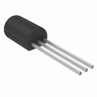
PACKAGE DIMENSIONS SEATING PLANE SECTION X− MPSW01, MPSW01A TO−92 (TO−226) CASE 29−10 ISSUE AL NOTES: 1. DIMENSIONING AND TOLERANCING PER ANSI ...

Related keywords