MMBT2222AWT1G ON Semiconductor, MMBT2222AWT1G Datasheet

TRANS GP SS NPN 40V SOT323

MMBT2222AWT1G

Manufacturer Part Number
MMBT2222AWT1G
Description
TRANS GP SS NPN 40V SOT323
Manufacturer
ON Semiconductor
Datasheet

Specifications of MMBT2222AWT1G

Transistor Type
NPN
Current - Collector (ic) (max)
600mA
Voltage - Collector Emitter Breakdown (max)
40V
Vce Saturation (max) @ Ib, Ic
1V @ 50mA, 500mA
Dc Current Gain (hfe) (min) @ Ic, Vce
100 @ 150mA, 10V
Power - Max
150mW
Frequency - Transition
300MHz
Mounting Type
Surface Mount
Package / Case
SC-70-3, SOT-323-3
Configuration
Single
Transistor Polarity
NPN
Mounting Style
SMD/SMT
Collector- Emitter Voltage Vceo Max
40 V
Emitter- Base Voltage Vebo
6 V
Continuous Collector Current
0.6 A
Maximum Dc Collector Current
0.6 A
Power Dissipation
150 mW
Maximum Operating Frequency
300 MHz
Maximum Operating Temperature
+ 150 C
Dc Collector/base Gain Hfe Min
35 at 0.1 mA at 10 V
Minimum Operating Temperature
- 55 C
Number Of Elements
1
Collector-emitter Voltage
40V
Collector-base Voltage
75V
Emitter-base Voltage
6V
Collector Current (dc) (max)
600mA
Frequency (max)
300MHz
Operating Temp Range
-55C to 150C
Operating Temperature Classification
Military
Mounting
Surface Mount
Pin Count
3
Package Type
SC-70
Lead Free Status / RoHS Status
Lead free / RoHS Compliant
Current - Collector Cutoff (max)
-
Lead Free Status / Rohs Status
Lead free / RoHS Compliant
Other names
MMBT2222AWT1GOS
MMBT2222AWT1GOS
MMBT2222AWT1GOSTR

Available stocks

Company
Part Number
Manufacturer
Quantity
Price
Part Number:
MMBT2222AWT1G
Manufacturer:
ON
Quantity:
360 000
Part Number:
MMBT2222AWT1G
Quantity:
18 000
Part Number:
MMBT2222AWT1G
Manufacturer:
ON
Quantity:
30 000
Part Number:
MMBT2222AWT1G
Manufacturer:
ON/安森美
Quantity:
20 000
Part Number:
MMBT2222AWT1G
Quantity:
24 000
Company:
Part Number:
MMBT2222AWT1G
Quantity:
39 000
MMBT2222AWT1
General Purpose Transistor
NPN Silicon
applications. They are housed in the SOT−323/SC−70 package which
is designed for low power surface mount applications.
Features
Stresses exceeding Maximum Ratings may damage the device. Maximum
Ratings are stress ratings only. Functional operation above the Recommended
Operating Conditions is not implied. Extended exposure to stresses above the
Recommended Operating Conditions may affect device reliability.
MAXIMUM RATINGS
© Semiconductor Components Industries, LLC, 2010
October, 2010 − Rev. 5
THERMAL CHARACTERISTICS
Collector −Emitter Voltage
Collector −Base Voltage
Emitter −Base Voltage
Collector Current − Continuous
Total Device Dissipation FR− 5 Board
Thermal Resistance, Junction−to−Ambient
Junction and Storage Temperature
These transistors are designed for general purpose amplifier
Compliant
These Devices are Pb−Free, Halogen Free/BFR Free and are RoHS
T
A
= 25°C
Characteristic
Rating
Symbol
Symbol
T
V
V
V
R
J
P
CEO
CBO
EBO
, T
I
qJA
C
D
stg
−55 to +150
Value
Max
600
150
833
6.0
40
75
1
mAdc
°C/W
Unit
Unit
Vdc
Vdc
Vdc
mW
°C
†For information on tape and reel specifications,
MMBT2222AWT1G
including part orientation and tape sizes, please
refer to our Tape and Reel Packaging Specification
Brochure, BRD8011/D.
*Date Code orientation may vary depending
upon manufacturing location.
(Note: Microdot may be in either location)
Device
1
ORDERING INFORMATION
P1 = Specific Device Code
M = Date Code*
G = Pb−Free Package
2
MARKING DIAGRAM
BASE
http://onsemi.com
1
3
1
COLLECTOR
(Pb−Free)
P1 M G
Package
EMITTER
SC−70
G
Publication Order Number:
3
2
CASE 419
STYLE 3
SC−70
MMBT2222AWT1/D
3000/Tape & Reel
Shipping

Related parts for MMBT2222AWT1G

MMBT2222AWT1G Summary of contents

Page 1

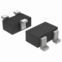
... Unit P 150 mW D 833 R °C/W qJA −55 to +150 °C J stg MMBT2222AWT1G †For information on tape and reel specifications, including part orientation and tape sizes, please refer to our Tape and Reel Packaging Specification Brochure, BRD8011/D. 1 http://onsemi.com COLLECTOR 3 1 BASE 2 EMITTER 3 SC−70 ...

Page 2

ELECTRICAL CHARACTERISTICS Characteristic OFF CHARACTERISTICS Collector −Emitter Breakdown Voltage (Note 1.0 mAdc Collector −Base Breakdown Voltage ( mAdc Emitter −Base Breakdown Voltage ( ...

Page 3

SWITCHING TIME EQUIVALENT TEST CIRCUITS 1.0 to 100 ms, DUTY CYCLE ≈ 2.0% + < Figure 1. Turn−On Time 1000 700 500 300 200 100 0.1 ...

Page 4

EB(off EB(off 7.0 5.0 3.0 2.0 5.0 7 100 I , COLLECTOR CURRENT (mA) C ...

Page 5

0.1 −55°C 25°C 0.01 0.001 0. COLLECTOR CURRENT (A) C Figure 11. Collector Emitter Saturation Voltage vs. Collector Current 1.2 1 1.0 0.9 −55°C 0.8 25°C ...

Page 6

... A1 *For additional information on our Pb−Free strategy and soldering details, please download the ON Semiconductor Soldering and Mounting Techniques Reference Manual, SOLDERRM/D. ON Semiconductor and are registered trademarks of Semiconductor Components Industries, LLC (SCILLC). SCILLC reserves the right to make changes without further notice to any products herein ...

Related keywords