STSA851 STMicroelectronics, STSA851 Datasheet
STSA851
Specifications of STSA851
Available stocks


Related parts for STSA851


STSA851 Summary of contents
Page 1
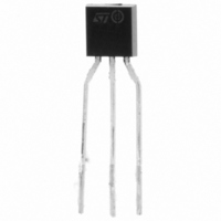
... Table 1. Device summary Order code Marking STSA851 SA851 STSA851-AP SA851 March 2008 TO-92 Figure 1. Internal schematic diagram Package TO-92 TO-92AP Rev 3 STSA851 TO-92AP Packaging Bulk Ammopack 1/11 www.st.com 11 ...
Page 2
... Contents 1 Electrical ratings . . . . . . . . . . . . . . . . . . . . . . . . . . . . . . . . . . . . . . . . . . . . 3 2 Electrical characteristics . . . . . . . . . . . . . . . . . . . . . . . . . . . . . . . . . . . . . 4 2.1 Electrical characteristics (curves 2.2 Test circuit . . . . . . . . . . . . . . . . . . . . . . . . . . . . . . . . . . . . . . . . . . . . . . . . . 6 3 Package mechanical data . . . . . . . . . . . . . . . . . . . . . . . . . . . . . . . . . . . . . 7 4 Revision history . . . . . . . . . . . . . . . . . . . . . . . . . . . . . . . . . . . . . . . . . . . 10 2/11 STSA851 ...
Page 3
... STSA851 Electrical ratings 1 Table 2. Absolute maximum rating Symbol V Collector-base voltage (I CBO V Collector-emitter voltage (I CEO V Emitter-base voltage (I EBO I Collector current C I Collector peak current ( Base current B P Total dissipation at T tot T Storage temperature stg T Max. operating junction temperature J Table 3. Thermal data Symbol ...
Page 4
... Test conditions V = 120 120 100 µ 100 µ 100 0 Min. Typ. Max 100 ° 150 120 140 200 200 mA 320 450 200 150 300 150 270 350 140 100 mA 130 MHz 1.35 120 STSA851 Unit nA 1 µ MHz pF ns µs ns ...
Page 5
... STSA851 2.1 Electrical characteristics (curves) Figure 2. Output characteristics Figure 4. Collector-emitter saturation voltage Figure 6. Base-emitter saturation voltage Electrical characteristics Figure 3. DC current gain Figure 5. Collector-emitter saturation voltage Figure 7. Base-emitter on voltage 5/11 ...
Page 6
... Electrical characteristics Figure 8. Switching times resistive load Figure 10. Capacitance 2.2 Test circuit Figure 11. Resistive load switching test circuit 1) Fast electronic switch 2) Non-inductive resistor 6/11 Figure 9. Switching times resistive load STSA851 ...
Page 7
... STSA851 3 Package mechanical data In order to meet environmental requirements, ST offers these devices in ECOPACK® packages. These packages have a Lead-free second level interconnect. The category of second level interconnect is marked on the package and on the inner box label, in compliance with JEDEC Standard JESD97. The maximum ratings related to soldering conditions are also marked on the inner box label ...
Page 8
... Package mechanical data DIM 8/11 TO-92 BULK SHIPMENT MECHANICAL DATA mm. MIN. TYP 4.32 0.36 4.45 3.30 2.41 1.14 12.70 2.16 0.92 0. STSA851 MAX. 4.95 0.51 4.95 3.94 2.67 1.40 15.49 2.41 1.52 0.56 0102782 C ...
Page 9
... STSA851 TO-92 AMMOPACK SHIPMENT (Suffix”-AP”) MECHANICAL DATA DIM F1,F2 delta delta P mm. MIN. TYP 12.50 12.70 5.65 6.35 2.44 2.54 -2.00 17.50 18.00 5.70 6.00 8.50 9.00 18.50 15.50 16.00 3.80 4.00 3.00 -1.00 Package mechanical data MAX. 4.80 3 ...
Page 10
... Revision history 4 Revision history Table 5. Document revision history Date 05-Sep-2003 25-Mar-2008 10/11 Revision 2 3 New graphics. STSA851 Changes ...
Page 11
... STSA851 Information in this document is provided solely in connection with ST products. STMicroelectronics NV and its subsidiaries (“ST”) reserve the right to make changes, corrections, modifications or improvements, to this document, and the products and services described herein at any time, without notice. All ST products are sold pursuant to ST’s terms and conditions of sale. ...