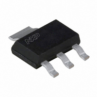
PBSS5540Z,115 NXP Semiconductors, PBSS5540Z,115 Datasheet - Page 3

PBSS5540Z,115
Manufacturer Part Number
PBSS5540Z,115
Description
TRANS PNP 40V 5A SOT223
Manufacturer
NXP Semiconductors
Datasheet
1.PBSS5540Z115.pdf
(9 pages)
Specifications of PBSS5540Z,115
Package / Case
SOT-223 (3 leads + Tab), SC-73, TO-261
Transistor Type
PNP
Current - Collector (ic) (max)
5A
Voltage - Collector Emitter Breakdown (max)
40V
Vce Saturation (max) @ Ib, Ic
160mV @ 200mA, 2A
Dc Current Gain (hfe) (min) @ Ic, Vce
150 @ 2A, 2V
Power - Max
2W
Frequency - Transition
120MHz
Mounting Type
Surface Mount
Minimum Operating Temperature
- 65 C
Configuration
Single Dual Collector
Transistor Polarity
PNP
Mounting Style
SMD/SMT
Collector- Emitter Voltage Vceo Max
40 V
Emitter- Base Voltage Vebo
6 V
Maximum Dc Collector Current
5 A
Power Dissipation
2000 mW
Maximum Operating Frequency
120 MHz
Maximum Operating Temperature
+ 150 C
Number Of Elements
1
Collector-emitter Voltage
40V
Collector-base Voltage
40V
Emitter-base Voltage
6V
Collector Current (dc) (max)
5A
Dc Current Gain (min)
250
Frequency (max)
120MHz
Operating Temp Range
-65C to 150C
Operating Temperature Classification
Military
Mounting
Surface Mount
Pin Count
3 +Tab
Package Type
SOT-223
Lead Free Status / RoHS Status
Lead free / RoHS Compliant
Current - Collector Cutoff (max)
-
Lead Free Status / Rohs Status
Lead free / RoHS Compliant
Other names
568-4172-2
934055496115
PBSS5540Z T/R
PBSS5540Z T/R
934055496115
PBSS5540Z T/R
PBSS5540Z T/R
Available stocks
Company
Part Number
Manufacturer
Quantity
Price
Part Number:
PBSS5540Z,115
Manufacturer:
NEXPERIA/安世
Quantity:
20 000
NXP Semiconductors
LIMITING VALUES
In accordance with the Absolute Maximum Rating System (IEC 60134).
Notes
1. Device mounted on a printed-circuit board, single-sided copper, tinplated, mounting pad for collector 1 cm
2. Device mounted on a printed-circuit board, single-sided copper, tinplated, mounting pad for collector 6 cm
THERMAL CHARACTERISTICS
Note
1. Device mounted on a printed-circuit board, single-sided copper, tinplated, mounting pad for collector 1 cm
2001 Sep 21
V
V
V
I
I
I
P
T
T
T
R
SYMBOL
SYMBOL
C
CM
BM
stg
j
amb
CBO
CEO
EBO
tot
40 V low V
th j-a
For other mounting conditions, see “Thermal considerations for SOT223 in the General Part of associated
Handbook”.
collector-base voltage
collector-emitter voltage
emitter-base voltage
collector current (DC)
peak collector current
peak base current
total power dissipation
storage temperature
junction temperature
operating ambient temperature
thermal resistance from junction to
ambient
CEsat
PARAMETER
PARAMETER
PNP transistor
open emitter
open base
open collector
T
T
in free air; note 1
amb
amb
≤ 25 °C; note 1
≤ 25 °C; note 2
3
CONDITIONS
CONDITIONS
−
−
−
−
−
−
−
−
−65
−
−65
MIN.
VALUE
92
−40
−40
−6
−5
−10
−2
1.35
2
+150
150
+150
PBSS5540Z
MAX.
Product data sheet
UNIT
K/W
V
V
V
A
A
A
W
W
°C
°C
°C
2
2
2
.
.
.
UNIT


