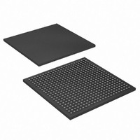
XC3SD3400A-4CSG484I Xilinx Inc, XC3SD3400A-4CSG484I Datasheet - Page 42

XC3SD3400A-4CSG484I
Manufacturer Part Number
XC3SD3400A-4CSG484I
Description
FPGA Spartan®-3A Family 3.4M Gates 53712 Cells 667MHz 90nm Technology 1.2V 484-Pin LCSBGA
Manufacturer
Xilinx Inc
Series
Spartan™-3A DSPr
Datasheets
1.XC3S50A-4VQG100C.pdf
(7 pages)
2.XC3SD3400A-4FGG676C.pdf
(4 pages)
3.XC3SD3400A-4FGG676C.pdf
(101 pages)
Specifications of XC3SD3400A-4CSG484I
Package
484LCSBGA
Family Name
Spartan®-3A
Device Logic Units
53712
Device System Gates
3400000
Maximum Internal Frequency
667 MHz
Typical Operating Supply Voltage
1.2 V
Maximum Number Of User I/os
309
Ram Bits
2322432
Number Of Logic Elements/cells
53712
Number Of Labs/clbs
5968
Total Ram Bits
2322432
Number Of I /o
309
Number Of Gates
3400000
Voltage - Supply
1.14 V ~ 1.26 V
Mounting Type
Surface Mount
Operating Temperature
-40°C ~ 100°C
Package / Case
484-FBGA, CSPBGA
No. Of Logic Blocks
5968
No. Of Gates
3400000
No. Of Macrocells
53712
Family Type
Spartan-3A
No. Of Speed Grades
4
No. Of I/o's
309
Clock Management
DCM
Rohs Compliant
Yes
Lead Free Status / RoHS Status
Lead free / RoHS Compliant
For Use With
122-1532 - KIT DEVELOPMENT SPARTAN 3ADSP
Lead Free Status / RoHS Status
Lead free / RoHS Compliant
Available stocks
Company
Part Number
Manufacturer
Quantity
Price
Company:
Part Number:
XC3SD3400A-4CSG484I
Manufacturer:
XILINX
Quantity:
380
Company:
Part Number:
XC3SD3400A-4CSG484I
Manufacturer:
Xilinx Inc
Quantity:
10 000
Company:
Part Number:
XC3SD3400A-4CSG484IL
Manufacturer:
XILINX
Quantity:
513
DSP48A Timing
To reference the DSP48A block diagram, see UG431: XtremeDSP DSP48A for Spartan-3A DSP FPGA User Guide.
Table 34: Setup Times for the DSP48A
DS610 (v3.0) October 4, 2010
Product Specification
Notes:
1.
2.
Setup Times of Data/Control Pins to the Input Register Clock
T
T
T
T
T
T
Setup Times of Data Pins to the Pipeline Register Clock
T
T
T
T
Setup Times of Data/Control Pins to the Output Register Clock
T
T
T
T
T
DSPDCK_AA
DSPDCK_DB
DSPDCK_CC
DSPDCK_DD
DSPDCK_OPB
DSPDCK_OPOP
DSPDCK_AM
DSPDCK_BM
DSPDCK_DM
DSPDCK_OPM
DSPDCK_AP
DSPDCK_BP
DSPDCK_DP
DSPDCK_CP
DSPDCK_OPP
Symbol
"Yes" means that the component is in the path. "No" means that the component is being bypassed. “–“ means that no path exists, so it is not
applicable.
The numbers in this table are based on the operating conditions set forth in
A input to A register CLK
D input to B register CLK
C input to C register CLK
D input to D register CLK
OPMODE input to B register CLK
OPMODE input to OPMODE register CLK
A input to M register CLK
B input to M register CLK
D input to M register CLK
OPMODE to M register CLK
A input to P register CLK
B input to P register CLK
D input to P register CLK
C input to P register CLK
OPMODE input to P register CLK
Description
Spartan-3A DSP FPGA Family: DC and Switching Characteristics
www.xilinx.com
Pre-adder
Yes
Yes
Yes
Yes
Yes
Yes
Yes
Yes
No
No
–
–
–
–
–
–
–
Table
Multiplier
Yes
Yes
Yes
Yes
Yes
Yes
Yes
Yes
Yes
Yes
–
–
–
–
–
–
–
7.
Post-adder
Yes
Yes
Yes
Yes
Yes
Yes
–
–
–
–
–
–
–
–
–
–
–
0.04
1.64
0.05
0.04
0.37
0.06
3.30
4.33
3.30
4.41
4.72
4.78
5.87
4.77
5.95
1.90
6.25
Min
-5
Speed Grade
0.04
1.88
0.05
0.04
0.42
0.06
3.79
4.97
3.79
5.06
5.42
5.49
6.74
5.48
6.83
2.18
7.18
Min
-4
Units
ns
ns
ns
ns
ns
ns
ns
ns
ns
ns
ns
ns
ns
ns
ns
ns
ns
42


