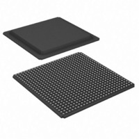
XC3S1400AN-5FGG676C Xilinx Inc, XC3S1400AN-5FGG676C Datasheet - Page 57

XC3S1400AN-5FGG676C
Manufacturer Part Number
XC3S1400AN-5FGG676C
Description
FPGA Spartan®-3AN Family 1.4M Gates 25344 Cells 770MHz 90nm Technology 1.2V 676-Pin FBGA
Manufacturer
Xilinx Inc
Series
Spartan™-3ANr
Datasheets
1.XC3S50A-4VQG100C.pdf
(7 pages)
2.XC3S50AN-4TQG144C.pdf
(2 pages)
3.XC3S50AN-4TQG144C.pdf
(123 pages)
Specifications of XC3S1400AN-5FGG676C
Package
676FBGA
Family Name
Spartan®-3AN
Device Logic Units
25344
Device System Gates
1400000
Maximum Internal Frequency
770 MHz
Typical Operating Supply Voltage
1.2 V
Maximum Number Of User I/os
502
Ram Bits
589824
Number Of Logic Elements/cells
25344
Number Of Labs/clbs
2816
Total Ram Bits
589824
Number Of I /o
502
Number Of Gates
1400000
Voltage - Supply
1.14 V ~ 1.26 V
Mounting Type
Surface Mount
Operating Temperature
0°C ~ 85°C
Package / Case
676-BBGA
Lead Free Status / RoHS Status
Lead free / RoHS Compliant
Other names
122-1600
XC3S1400AN-5FGG676C
XC3S1400AN-5FGG676C
Available stocks
Company
Part Number
Manufacturer
Quantity
Price
Company:
Part Number:
XC3S1400AN-5FGG676C
Manufacturer:
XILINX
Quantity:
490
Company:
Part Number:
XC3S1400AN-5FGG676C
Manufacturer:
Xilinx Inc
Quantity:
10 000
DNA Port Timing
Table 46: DNA_PORT Interface Timing
Internal SPI Access Port Timing
Table 47: SPI_ACCESS Interface Timing
DS557 (v4.1) April 1, 2011
Product Specification
Notes:
1.
Notes:
1.
T
T
T
T
T
SPICCK_MOSI
SPICKC_MOSI
SPICKO_MISO
T
T
SPICCK_CSB
SPICCK_CSB
T
T
The minimum READ pulse width is 5 ns, the maximum READ pulse width is 10 µ
For details on using SPI_ACCESS and the In-System Flash memory, see
F
F
T
T
T
T
T
Symbol
Symbol
T
T
F
T
DNADCKO
DNACLKH
DNACLKF
DNACLKL
DNADSU
DNARSU
SPICAR1
SPICAR1
SPICLKH
DNASSU
SPICLKL
DNADH
DNARH
T
SPICLK
DNASH
CSB
Setup time on SHIFT before the rising edge of CLK
Hold time on SHIFT after the rising edge of CLK
Setup time on DIN before the rising edge of CLK
Hold time on DIN after the rising edge of CLK
Setup time on READ before the rising edge of CLK
Hold time on READ after the rising edge of CLK
Clock-to-output delay on DOUT after rising edge of CLK
CLK frequency
CLK High time
CLK Low time
Setup time on MOSI before the active edge of CLK
Hold time on MOSI after the active edge of CLK
CSB High time
Setup time on CSB before the active edge of CLK
Hold time on CSB after the active edge of CLK
Clock-to-output delay on MISO after active edge of CLK
CLK frequency
CLK frequency for Continuous Array Read command
CLK frequency for Continuous Array Read command,
reduced initial latency
CLK High time
CLK Low time
Description
Description
www.xilinx.com
Spartan-3AN FPGA Family: DC and Switching Characteristics
UG333
s
.
Spartan-3AN FPGA In-System Flash User Guide.
4.47
4.03
7.15
7.15
Min
6.8
50
–
–
–
–
–
-5
Max
14.3
Speed Grade
50
50
33
–
–
–
–
–
Min
1.0
0.5
1.0
0.5
5.0
0.5
1.0
1.0
0
0
Min
5.0
4.5
8.0
8.0
6.8
50
–
–
–
–
–
10,000
Max
100
-4
1.5
–
–
–
–
–
Max
16.0
50
50
33
–
–
–
–
–
Units
MHz
ns
ns
ns
ns
ns
ns
ns
ns
ns
Units
MHz
MHz
MHz
ns
ns
ns
ns
ns
ns
ns
ns
57


