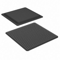
XC3S1400AN-5FGG676C Xilinx Inc, XC3S1400AN-5FGG676C Datasheet - Page 13

XC3S1400AN-5FGG676C
Manufacturer Part Number
XC3S1400AN-5FGG676C
Description
FPGA Spartan®-3AN Family 1.4M Gates 25344 Cells 770MHz 90nm Technology 1.2V 676-Pin FBGA
Manufacturer
Xilinx Inc
Series
Spartan™-3ANr
Datasheets
1.XC3S50A-4VQG100C.pdf
(7 pages)
2.XC3S50AN-4TQG144C.pdf
(2 pages)
3.XC3S50AN-4TQG144C.pdf
(123 pages)
Specifications of XC3S1400AN-5FGG676C
Package
676FBGA
Family Name
Spartan®-3AN
Device Logic Units
25344
Device System Gates
1400000
Maximum Internal Frequency
770 MHz
Typical Operating Supply Voltage
1.2 V
Maximum Number Of User I/os
502
Ram Bits
589824
Number Of Logic Elements/cells
25344
Number Of Labs/clbs
2816
Total Ram Bits
589824
Number Of I /o
502
Number Of Gates
1400000
Voltage - Supply
1.14 V ~ 1.26 V
Mounting Type
Surface Mount
Operating Temperature
0°C ~ 85°C
Package / Case
676-BBGA
Lead Free Status / RoHS Status
Lead free / RoHS Compliant
Other names
122-1600
XC3S1400AN-5FGG676C
XC3S1400AN-5FGG676C
Available stocks
Company
Part Number
Manufacturer
Quantity
Price
Company:
Part Number:
XC3S1400AN-5FGG676C
Manufacturer:
XILINX
Quantity:
490
Company:
Part Number:
XC3S1400AN-5FGG676C
Manufacturer:
Xilinx Inc
Quantity:
10 000
Power Supply Specifications
Table 7: Supply Voltage Thresholds for Power-On Reset
Table 8: Supply Voltage Ramp Rate
Table 9: Supply Voltage Levels Necessary for Preserving CMOS Configuration Latch (CCL) Contents and RAM Data
DS557 (v4.1) April 1, 2011
Product Specification
Notes:
1.
2.
Notes:
1.
2.
When configuring from the In-System Flash, V
reaches at least 3.0V before INIT_B goes High to indicate the start of configuration. V
be applied in any order if this requirement is met. However, an external configuration source might have specific requirements. Check the
data sheet for the attached configuration source. Apply V
Spartan-3 Generation FPGAs” in
To ensure successful power-on, V
no dips at any point.
Symbol
V
V
DRAUX
V
DRINT
V
Symbol
Symbol
V
V
V
V
CCAUXT
CCAUXR
CCINTR
CCINTT
CCO2T
CCO2R
V
V
CCINT
CCAUX
Threshold for the V
Threshold for the V
Threshold for the V
Ramp rate from GND to valid V
Ramp rate from GND to valid V
Ramp rate from GND to valid V
level required to retain CMOS Configuration Latch (CCL) and RAM data
level required to retain CMOS Configuration Latch (CCL) and RAM data
CCINT
CCINT
UG331
UG331
, V
, V
for more information).
CCO
for more information).
CCINT
CCAUX
CCO
CCO
Bank 2, and V
Bank 2, and V
CCAUX
CCAUX
Bank 2 supply
Description
Description
supply
supply
must be in the recommended operating range; on power-up make sure V
must be in the recommended operating range; on power-up make sure V
CCINT
CCAUX
CCO
Description
CCINT
CCINT
www.xilinx.com
Bank 2 supply level
CCAUX
CCAUX
supply level
Spartan-3AN FPGA Family: DC and Switching Characteristics
supply level
last for lowest overall power consumption (see the chapter called “Powering
last for lowest overall power consumption (see the chapter called “Powering
supplies must rise through their respective threshold-voltage ranges with
supplies must rise through their respective threshold-voltage ranges with
CCINT
CCINT
, V
, V
CCAUX
CCAUX
Min
Min
0.4
1.0
1.0
0.2
0.2
0.2
, and V
, and V
CCO
CCO
Max
Max
100
100
100
supplies to the FPGA can
1.0
2.0
2.0
supplies to the FPGA can
Min
1.0
2.0
CCAUX
CCAUX
Units
Units
Units
ms
ms
ms
V
V
V
V
V
13


