MBT3946DW1T1 ON Semiconductor, MBT3946DW1T1 Datasheet - Page 3
MBT3946DW1T1
Manufacturer Part Number
MBT3946DW1T1
Description
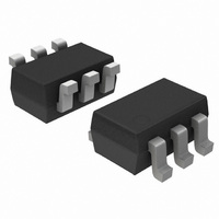
TRANS DUAL GP 200MA 40V SOT363
Manufacturer
ON Semiconductor
Datasheet
1.MBT3946DW1T1G.pdf
(10 pages)
Specifications of MBT3946DW1T1
Transistor Type
NPN, PNP
Current - Collector (ic) (max)
200mA
Voltage - Collector Emitter Breakdown (max)
40V
Vce Saturation (max) @ Ib, Ic
300mV @ 5mA, 50mA / 400mV @ 5mA, 50mA
Dc Current Gain (hfe) (min) @ Ic, Vce
100 @ 10mA, 1V
Power - Max
150mW
Frequency - Transition
300MHz, 250MHz
Mounting Type
Surface Mount
Package / Case
SC-70-6, SC-88, SOT-363
Dc
0534
Lead Free Status / RoHS Status
Contains lead / RoHS non-compliant
Current - Collector Cutoff (max)
-
Other names
MBT3946DW1T1OSCT
Available stocks
Company
Part Number
Manufacturer
Quantity
Price
Company:

Part Number:
MBT3946DW1T1
Manufacturer:
ON
Quantity:
440
Company:
Part Number:
MBT3946DW1T1
Manufacturer:
panasoni
Quantity:
12 000
Part Number:
MBT3946DW1T1
Manufacturer:
ON/安森美
Quantity:
20 000
Company:
Part Number:
MBT3946DW1T1G
Manufacturer:
ON
Quantity:
22 932
Company:
Part Number:
MBT3946DW1T1G
Manufacturer:
ON
Quantity:
30 000
Part Number:
MBT3946DW1T1G
Manufacturer:
ON/安森美
Quantity:
20 000


- 0.5 V
ELECTRICAL CHARACTERISTICS
SWITCHING CHARACTERISTICS
Output Admittance
(V
(V
Noise Figure
(V
(V
Delay Time
Rise Time
Storage Time
Fall Time
DUTY CYCLE = 2%
300 ns
CE
CE
CE
CE
7.0
5.0
3.0
2.0
1.0
10
0.1
= 10 Vdc, I
= −10 Vdc, I
= 5.0 Vdc, I
= −5.0 Vdc, I
0.2 0.3 0.5 0.7
Figure 1. Delay and Rise Time
C
Equivalent Test Circuit
C
(V
(V
(I
(I
(V
(V
(I
(I
C
C
= 1.0 mAdc, f = 1.0 kHz)
C
C
B1
B1
= 100 mAdc, R
CC
CC
CC
CC
= −1.0 mAdc, f = 1.0 kHz)
REVERSE BIAS VOLTAGE (VOLTS)
= −100 mAdc, R
= 10 mAdc, I
= −10 mAdc, I
= I
= I
Figure 3. Capacitance
= 3.0 Vdc, V
= −3.0 Vdc, V
= 3.0 Vdc, I
= −3.0 Vdc, I
B2
B2
+10.9 V
< 1 ns
= 1.0 mAdc)
= −1.0 mAdc)
1.0
C
ibo
10 k
B1
S
C
Characteristic
C
2.0 3.0 5.0 7.0 10
B1
obo
BE
= 1.0 kW, f = 1.0 kHz)
C
S
= 1.0 mAdc)
= 10 mAdc)
BE
= −1.0 mAdc)
= −10 mAdc)
= 1.0 kW, f = 1.0 kHz)
= − 0.5 Vdc)
= 0.5 Vdc)
(NPN)
TYPICAL TRANSIENT CHARACTERISTICS
(T
* Total shunt capacitance of test jig and connectors
A
= 25°C unless otherwise noted) (Continued)
+3 V
275
C
20 30 40
s
http://onsemi.com
< 4 pF*
DUTY CYCLE = 2%
10 < t
(NPN)
1
3
< 500 ms
T
T
J
J
= 25°C
= 125°C
5000
3000
2000
1000
700
500
300
200
100
70
50
0
(NPN)
(NPN)
- 9.1 V′
(PNP)
(PNP)
(NPN)
(NPN)
(NPN)
(NPN)
(PNP)
(PNP)
(PNP)
(PNP)
1.0
V
I
C
CC
/I
t
B
1
= 40 V
2.0 3.0
= 10
Figure 2. Storage and Fall Time
Symbol
h
NF
t
t
t
t
oe
+10.9 V
d
s
Equivalent Test Circuit
r
f
I
C
Figure 4. Charge Data
, COLLECTOR CURRENT (mA)
5.0 7.0 10
< 1 ns
Min
1.0
3.0
1N916
10 k
−
−
−
−
−
−
−
−
−
−
20
Q
(NPN)
T
30
Max
200
225
5.0
4.0
40
60
35
35
35
35
50
75
50 70 100
+3 V
Q
A
275
mmhos
C
Unit
s
dB
ns
ns
< 4 pF*
200
Related parts for MBT3946DW1T1
Image
Part Number
Description
Manufacturer
Datasheet
Request
R

Part Number:
Description:
ON Semiconductor [VOLTAGE REGULATOR]
Manufacturer:
ON Semiconductor
Datasheet:
Part Number:
Description:
357-036-542-201 CARDEDGE 36POS DL .156 BLK LOPRO
Manufacturer:
ON Semiconductor
Datasheet:
Part Number:
Description:
357-036-542-201 CARDEDGE 36POS DL .156 BLK LOPRO
Manufacturer:
ON Semiconductor
Datasheet:
Part Number:
Description:
357-036-542-201 CARDEDGE 36POS DL .156 BLK LOPRO
Manufacturer:
ON Semiconductor
Datasheet:
Part Number:
Description:
357-036-542-201 CARDEDGE 36POS DL .156 BLK LOPRO
Manufacturer:
ON Semiconductor
Datasheet:
Part Number:
Description:
357-036-542-201 CARDEDGE 36POS DL .156 BLK LOPRO
Manufacturer:
ON Semiconductor
Datasheet:
Part Number:
Description:
357-036-542-201 CARDEDGE 36POS DL .156 BLK LOPRO
Manufacturer:
ON Semiconductor
Datasheet:
Part Number:
Description:
357-036-542-201 CARDEDGE 36POS DL .156 BLK LOPRO
Manufacturer:
ON Semiconductor
Datasheet:
Part Number:
Description:
357-036-542-201 CARDEDGE 36POS DL .156 BLK LOPRO
Manufacturer:
ON Semiconductor
Datasheet:
Part Number:
Description:
357-036-542-201 CARDEDGE 36POS DL .156 BLK LOPRO
Manufacturer:
ON Semiconductor
Datasheet:
Part Number:
Description:
357-036-542-201 CARDEDGE 36POS DL .156 BLK LOPRO
Manufacturer:
ON Semiconductor
Datasheet:
Part Number:
Description:
Manufacturer:
ON Semiconductor
Datasheet:
Part Number:
Description:
Manufacturer:
ON Semiconductor
Datasheet:
Part Number:
Description:
Manufacturer:
ON Semiconductor
Datasheet: