MCR08BT1 ON Semiconductor, MCR08BT1 Datasheet
MCR08BT1
Specifications of MCR08BT1
Available stocks


Related parts for MCR08BT1

MCR08BT1 Summary of contents
Page 1
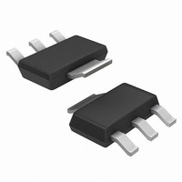
... Microdot may be in either location) PIN ASSIGNMENT 1 Cathode 2 Anode 3 Gate 4 Anode ORDERING INFORMATION Device Package Shipping SOT−223 1000/Tape &Reel SOT−223 1000/Tape &Reel (Pb−Free) SOT−223 1000/Tape & Reel SOT−223 1000/Tape & Reel (Pb−Free) Publication Order Number: MCR08BT1/D † ...
Page 2
ELECTRICAL CHARACTERISTICS Characteristic OFF CHARACTERISTICS Peak Repetitive Forward or Reverse Blocking Current (Note Rated DRM RRM GK ON CHARACTERISTICS Peak Forward On-State Voltage (Note 2) (I Gate Trigger ...
Page 3
INSTANTANEOUS ON‐STATE VOLTAGE (VOLTS) T Figure 2. On-State Characteristics 110 100 HALFWAVE 0.1 0.2 ...
Page 4
CONDUCTION 60 ANGLE 0.7 0.6 90 0.5 0.4 0.3 0.2 120 0 0.1 0.2 0 AVERAGE ON‐STATE CURRENT (AMPS) T(AV) Figure 8. Power Dissipation 0.7 0.6 0.5 0.4 0.3 -40 -20 ...
Page 5
I GT 1.0 0.1 1.0 10 100 1000 R , GATE‐CATHODE RESISTANCE (OHMS) GK Figure 14. Holding Current Range versus Gate-Cathode Resistance 10000 300 V 1000 200 V 500 400 V 100 50 500 V ...
Page 6
... − − 2. ANODE 3. GATE 4. ANODE ON Semiconductor Website: http://onsemi.com Order Literature: http://www.onsemi.com/litorder For additional information, please contact your local Sales Representative. MCR08BT1/D MAX 0.068 0.004 0.035 0.126 0.014 0.263 0.145 0.094 0.041 0.078 0.287 10 ...