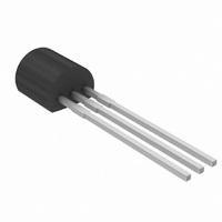
EC103D1,412 NXP Semiconductors, EC103D1,412 Datasheet

EC103D1,412
Specifications of EC103D1,412
Related parts for EC103D1,412
EC103D1,412 Summary of contents
Page 1
EC103D1 Thyristor, sensitive gate Rev. 02 — 31 July 2008 1. Product profile 1.1 General description Passivated ultra sensitive gate thyristor in a SOT54 plastic package. 1.2 Features I Ultra sensitive gate 1.3 Applications I Earth leakage circuit breakers or ...
Page 2
... NXP Semiconductors 3. Ordering information Table 2. Ordering information Type number Package Name EC103D1 TO-92 4. Limiting values Table 3. Limiting values In accordance with the Absolute Maximum Rating System (IEC 60134). Symbol Parameter V repetitive peak off-state voltage DRM V repetitive peak reverse voltage RRM V non-repetitive peak off-state voltage ...
Page 3
... NXP Semiconductors 0.6 P tot (W) 0.4 0.2 0.0 0.0 0.1 Form factor T(RMS) T(AV) Fig 1. Total power dissipation as a function of average on-state current; maximum values 10 I TSM ( Fig 2. Non-repetitive peak on-state current as a function of the number of sinusoidal current cycles; maximum values EC103D1_2 Product data sheet 2 ...
Page 4
... NXP Semiconductors TSM ( Fig 3. Non-repetitive peak on-state current as a function of pulse duration; maximum values 12 I T(RMS) ( lead Fig 4. RMS on-state current as a function of surge duration; maximum values EC103D1_2 Product data sheet -4 10 003aaa117 I T(RMS) (A) 0.8 0.6 0.4 0 surge duration (s) Fig 5. Rev. 02 — 31 July 2008 ...
Page 5
... NXP Semiconductors 5. Thermal characteristics Table 4. Thermal characteristics Symbol Parameter R thermal resistance from junction to th(j-lead) lead R thermal resistance from junction to th(j-a) ambient th(j-lead) (K/ Fig 6. Transient thermal impedance from junction to lead as a function of pulse duration EC103D1_2 Product data sheet Conditions see Figure 6 printed-circuit board mounted ...
Page 6
... NXP Semiconductors 6. Characteristics Table 5. Characteristics unless otherwise stated. j Symbol Parameter Static characteristics I gate trigger current GT I latching current L I holding current H V on-state voltage T V gate trigger voltage GT I off-state current D I reverse current R Dynamic characteristics dV /dt rate of rise of off-state D voltage ...
Page 7
... NXP Semiconductors 1 GT(25 C) 1.2 0.8 0 Fig 7. Normalized gate trigger voltage as a function of junction temperature 2 (A) 2.0 1.5 1.0 (1) 0.5 0 0.4 0 0.895 0.195 s ( 125 C; typical values j ( 125 C; maximum values j ( typical values j Fig 9. On-state current as a function of on-state voltage EC103D1_2 Product data sheet ...
Page 8
... NXP Semiconductors 2 H(25 C) 1.6 1.2 0.8 0 Fig 11. Normalized holding current as a function of junction temperature 7. Package information Epoxy meets requirements V-0 at 3.175 mm EC103D1_2 Product data sheet 003aaa115 / 100 150 (1) R Fig 12. Critical rate of rise of off-state voltage as a function of junction temperature; typical values Rev. 02 — ...
Page 9
... NXP Semiconductors 8. Package outline Plastic single-ended leaded (through hole) package; 3 leads DIMENSIONS (mm are the original dimensions) UNIT 5.2 0.48 0.66 0.45 mm 5.0 0.40 0.55 0.38 Note 1. Terminal dimensions within this zone are uncontrolled to allow for flow of plastic and terminal irregularities. OUTLINE ...
Page 10
... Release date EC103D1_2 20080731 • Modifications: The format of this data sheet has been redesigned to comply with the new identity guidelines of NXP Semiconductors. • Legal texts have been adapted to the new company name where appropriate. • Table 3 “Limiting values” on page • ...
Page 11
... Right to make changes — NXP Semiconductors reserves the right to make changes to information published in this document, including without limitation specifications and product descriptions, at any time and without notice ...
Page 12
... NXP Semiconductors 12. Contents 1 Product profi 1.1 General description 1.2 Features . . . . . . . . . . . . . . . . . . . . . . . . . . . . . . 1 1.3 Applications . . . . . . . . . . . . . . . . . . . . . . . . . . . 1 1.4 Quick reference data Pinning information . . . . . . . . . . . . . . . . . . . . . . 1 3 Ordering information . . . . . . . . . . . . . . . . . . . . . 2 4 Limiting values Thermal characteristics Characteristics . . . . . . . . . . . . . . . . . . . . . . . . . . 6 7 Package information . . . . . . . . . . . . . . . . . . . . . 8 8 Package outline . . . . . . . . . . . . . . . . . . . . . . . . . 9 9 Revision history . . . . . . . . . . . . . . . . . . . . . . . . 10 10 Legal information 10.1 Data sheet status ...


