C106BG ON Semiconductor, C106BG Datasheet - Page 2
C106BG
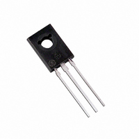
Manufacturer Part Number
C106BG
Description
THYRISTOR SCR 4A 200V TO225AA
Manufacturer
ON Semiconductor
Specifications of C106BG
Scr Type
Sensitive Gate
Voltage - Off State
200V
Voltage - Gate Trigger (vgt) (max)
800mV
Voltage - On State (vtm) (max)
2.2V
Current - On State (it (av)) (max)
2.55A
Current - On State (it (rms)) (max)
4A
Current - Gate Trigger (igt) (max)
200µA
Current - Hold (ih) (max)
3mA
Current - Off State (max)
10µA
Current - Non Rep. Surge 50, 60hz (itsm)
20A @ 60Hz
Operating Temperature
-40°C ~ 110°C
Mounting Type
Through Hole
Package / Case
TO-225-3
Current - On State (it (rms) (max)
4A
Current Squared Time Rating
1.65
Current, Forward
4 A
Current, Surge
20 A
Package Type
TO-225AA
Primary Type
SCR
Resistance, Thermal, Junction To Case
3 °C/W
Temperature, Junction, Maximum
+110 °C
Temperature, Operating
-40 to +110 °C
Voltage, Forward
2.2 V
Voltage, Reverse
200 V
Lead Free Status / RoHS Status
Lead free / RoHS Compliant
Other names
C106BGOS


Stresses exceeding Maximum Ratings may damage the device. Maximum Ratings are stress ratings only. Functional operation above the
Recommended Operating Conditions is not implied. Extended exposure to stresses above the Recommended Operating Conditions may affect
device reliability.
1. V
2. Torque rating applies with use of compression washer (B52200F006). Mounting torque in excess of 6 in. lb. does not appreciably lower
†For information on tape and reel specifications, including part orientation and tape sizes, please refer to our Tape and Reel Packaging
*D1 signifies European equivalent for D suffix and M1 signifies European equivalent for M suffix.
MAXIMUM RATINGS
THERMAL CHARACTERISTICS
ORDERING INFORMATION
Specifications Brochure, BRD8011/D.
Peak Repetitive Off−State Voltage (Note 1)
On-State RMS Current
Average On−State Current
Peak Non-Repetitive Surge Current
Circuit Fusing Considerations (t = 8.3 ms)
Forward Peak Gate Power
Forward Average Gate Power
Forward Peak Gate Current
Operating Junction Temperature Range
Storage Temperature Range
Mounting Torque (Note 2)
Thermal Resistance, Junction−to−Case
Thermal Resistance, Junction−to−Ambient
Maximum Lead Temperature for Soldering Purposes 1/8 in. from Case for 10 Seconds
C106B
C106BG
C106D
C106DG
C106D1*
C106D1G*
C106M
C106MG
C106M1*
C106M1G*
voltage shall not be applied concurrent with negative potential on the anode. Blocking voltages shall not be tested with a constant current
source such that the voltage ratings of the devices are exceeded.
case-to-sink thermal resistance. Anode lead and heatsink contact pad are common.
(Sine Wave, 50−60 Hz, R
T
(180° Conduction Angles, T
(180° Conduction Angles, T
(1/2 Cycle, Sine Wave, 60 Hz, T
(Pulse Width v1.0 msec, T
(Pulse Width v1.0 msec, T
(Pulse Width v1.0 msec, T
DRM
C
= −40° to 110°C)
and V
RRM
for all types can be applied on a continuous basis. Ratings apply for zero or negative gate voltage; however, positive gate
Device
(T
J
= 25°C unless otherwise noted)
GK
C
C
C
C
C
= 1 kW,
= 80°C)
= 80°C)
= 80°C)
= 80°C)
= 80°C)
J
Characteristic
= +110°C)
Characteristic
(T
C
= 25°C unless otherwise noted.)
http://onsemi.com
C106B
C106D, C106D1*
C106M, C106M1*
TO−225AA
TO−225AA
TO−225AA
TO−225AA
TO−225AA
TO−225AA
TO−225AA
TO−225AA
TO−225AA
TO−225AA
(Pb−Free)
(Pb−Free)
(Pb−Free)
(Pb−Free)
(Pb−Free)
Package
2
Symbol
R
R
T
qJC
qJA
L
Symbol
I
V
P
V
T(RMS)
I
I
P
T(AV)
I
T
DRM,
TSM
G(AV)
RRM
I
GM
T
GM
stg
2
−
J
t
500 Units / Box
500 Units / Box
500 Units / Box
500 Units / Box
500 Units / Box
500 Units / Box
500 Units / Box
500 Units / Box
500 Units / Box
500 Units / Box
Max
260
3.0
Shipping
75
−40 to +110
−40 to +150
Max
2.55
1.65
200
400
600
4.0
0.5
0.1
0.2
6.0
20
†
°C/W
°C/W
Unit
°C
in. lb.
Unit
A
°C
°C
W
W
V
A
A
A
A
2
s
Related parts for C106BG
Image
Part Number
Description
Manufacturer
Datasheet
Request
R

Part Number:
Description:
SCRs 200V 4A
Manufacturer:
ON Semiconductor
Datasheet:

Part Number:
Description:
Sensitive Gate Silicon Controlled Rectifiers
Manufacturer:
ON Semiconductor
Datasheet:
Part Number:
Description:
ON Semiconductor [VOLTAGE REGULATOR]
Manufacturer:
ON Semiconductor
Datasheet:
Part Number:
Description:
357-036-542-201 CARDEDGE 36POS DL .156 BLK LOPRO
Manufacturer:
ON Semiconductor
Datasheet:
Part Number:
Description:
357-036-542-201 CARDEDGE 36POS DL .156 BLK LOPRO
Manufacturer:
ON Semiconductor
Datasheet:
Part Number:
Description:
357-036-542-201 CARDEDGE 36POS DL .156 BLK LOPRO
Manufacturer:
ON Semiconductor
Datasheet:
Part Number:
Description:
357-036-542-201 CARDEDGE 36POS DL .156 BLK LOPRO
Manufacturer:
ON Semiconductor
Datasheet:
Part Number:
Description:
357-036-542-201 CARDEDGE 36POS DL .156 BLK LOPRO
Manufacturer:
ON Semiconductor
Datasheet:
Part Number:
Description:
357-036-542-201 CARDEDGE 36POS DL .156 BLK LOPRO
Manufacturer:
ON Semiconductor
Datasheet:
Part Number:
Description:
357-036-542-201 CARDEDGE 36POS DL .156 BLK LOPRO
Manufacturer:
ON Semiconductor
Datasheet:
Part Number:
Description:
357-036-542-201 CARDEDGE 36POS DL .156 BLK LOPRO
Manufacturer:
ON Semiconductor
Datasheet:
Part Number:
Description:
357-036-542-201 CARDEDGE 36POS DL .156 BLK LOPRO
Manufacturer:
ON Semiconductor
Datasheet:
Part Number:
Description:
357-036-542-201 CARDEDGE 36POS DL .156 BLK LOPRO
Manufacturer:
ON Semiconductor
Datasheet:
Part Number:
Description:
Manufacturer:
ON Semiconductor
Datasheet: