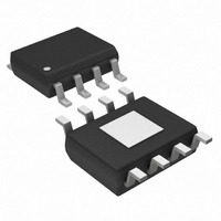
MAX2601ESA+T Maxim Integrated Products, MAX2601ESA+T Datasheet - Page 3

MAX2601ESA+T
Manufacturer Part Number
MAX2601ESA+T
Description
TRANS RF NPN 900MHZ 15V 8SOIC
Manufacturer
Maxim Integrated Products
Datasheet
1.MAX2601ESAT.pdf
(6 pages)
Specifications of MAX2601ESA+T
Transistor Type
NPN
Voltage - Collector Emitter Breakdown (max)
15V
Frequency - Transition
1GHz
Noise Figure (db Typ @ F)
3.3dB @ 836MHz
Gain
11.6dB
Power - Max
6.4W
Dc Current Gain (hfe) (min) @ Ic, Vce
100 @ 250mA, 3V
Current - Collector (ic) (max)
1.2A
Mounting Type
Surface Mount
Package / Case
8-SOIC (3.9mm Width) Exposed Pad, 8-eSOIC. 8-HSOIC
Lead Free Status / RoHS Status
Lead free / RoHS Compliant
(Test Circuit of Figure 1, input/output matching networks optimized for specific measurement frequency, V
P
__________________________________________Typical Operating Characteristics
______________________________________________________________Pin Description
OUT
1.0
0.8
0.6
0.4
0.2
35
25
15
-5
0
5
2, 3, 6, 7, Slug
= 30dBm, Z
0
5
MAX2601
TWO-TONE OUTPUT POWER, IM3, IM5
P
ARE RMS COMPOSITE
TWO-TONE
POWER LEVELS
OUT
1, 8
4, 5
vs. INPUT POWER (f = 433MHz)
—
, IM3, AND IM5
1
COLLECTOR CURRENT
10
V
INPUT POWER (dBm)
2
BB
V
LOAD
BB
= 0.85V
= 1.00V
_______________________________________________________________________________________
V
CE
PIN
3
15
V
(V)
= Z
BB
= 0.95V
IM5
SOURCE
IM3
P
4
OUT
V
2, 6, 7, Slug
BB
20
MAX2602
V
BB
= 0.80V
5
= 0.90V
1, 8
4, 5
3
= 50Ω, f = 836MHz, T
25
6
-20
-22
-24
-26
-28
-30
-32
-34
-36
-38
-40
31
30
29
28
27
3.6V, 1W RF Power Transistors
(IS-54 π/4 DQPSK MODULATION, V
NAME
0.4
10
BIAS
C
TWO-TONE OUTPUT POWER AND IM3
E
B
P
ARE RMS COMPOSITE
TWO-TONE POWER LEVELS
OUT
, IM3, AND IM5
ACPR vs. OUTPUT POWER
15
vs. COLLECTOR CURRENT
A
0.5
= +25°C, unless otherwise noted.)
Transistor Collector
Transistor Emitter
Anode of the Biasing Diode that matches the thermal and process char-
acteristics of the power transistor. Requires a high-RF-impedance, low-
DC-impedance (e.g., inductor) connection to the transistor base (Pin 4).
Current through the biasing diode (into Pin 3) is proportional to 1/15 the
collector current in the transistor.
Transistor Base
OUTPUT POWER (dBm)
20
for 900MHz Applications
I
CC
3.6V
0.6
(A)
3.0V
25
4.8V
P
0.7
OUT
30
BB
4.2V
IM3
= 0.85V)
0.8
35
20
19
18
17
16
FUNCTION
50
40
30
20
10
35
25
15
60
-5
5
0
(IS-54 π/4 DQPSK MODULATION, V
COLLECTOR EFFICIENCY vs. OUTPUT POWER
10
5
TWO-TONE OUTPUT POWER, IM3, IM5
P
ARE RMS COMPOSITE
TWO-TONE POWER
LEVELS
P
ARE RMS COMPOSITE
TWO-TONE POWER
LEVELS
OUT
OUT
, IM3, AND IM5
, IM3, AND IM5
15
CC
10
OUTPUT POWER (dBm)
vs. INPUT POWER
INPUT POWER (dBm)
3.6V
= 3.6V, V
3.0V
20
15
25
BB
IM3
P
IM5
OUT
4.8V
= 0.750V,
20
4.2V
30
BB
= 0.85V)
25
35
3


