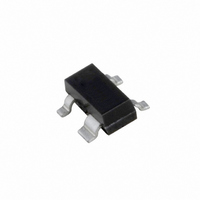
BFG520/XR,215 NXP Semiconductors, BFG520/XR,215 Datasheet - Page 3

BFG520/XR,215
Manufacturer Part Number
BFG520/XR,215
Description
TRANS NPN 6V 70MA SOT143B
Manufacturer
NXP Semiconductors
Datasheet
1.BFG520X215.pdf
(14 pages)
Specifications of BFG520/XR,215
Package / Case
SOT-143, SOT-143B, TO-253AA
Mounting Type
Surface Mount
Power - Max
300mW
Current - Collector (ic) (max)
70mA
Voltage - Collector Emitter Breakdown (max)
15V
Transistor Type
NPN
Frequency - Transition
9GHz
Dc Current Gain (hfe) (min) @ Ic, Vce
60 @ 20mA, 6V
Noise Figure (db Typ @ F)
1.6dB ~ 2.1dB @ 900MHz
Dc Collector/base Gain Hfe Min
60
Mounting Style
SMD/SMT
Configuration
Dual
Transistor Polarity
NPN
Collector- Emitter Voltage Vceo Max
15 V
Emitter- Base Voltage Vebo
2.5 V
Continuous Collector Current
70 mA
Power Dissipation
300 mW
Lead Free Status / RoHS Status
Lead free / RoHS Compliant
Gain
-
Lead Free Status / Rohs Status
Lead free / RoHS Compliant
Other names
934018820215::BFG520/XR T/R::BFG520/XR T/R
NXP Semiconductors
LIMITING VALUES
In accordance with the Absolute Maximum System (IEC 134).
THERMAL RESISTANCE
Note
1. T
V
V
V
I
P
T
T
R
C
stg
j
CBO
CEO
EBO
tot
th j-s
NPN 9 GHz wideband transistor
SYMBOL
s
SYMBOL
is the temperature at the soldering point of the collector tab.
collector-base voltage
collector-emitter voltage
emitter-base voltage
DC collector current
total power dissipation
storage temperature
junction temperature
thermal resistance from junction to
soldering point
PARAMETER
PARAMETER
Rev. 04 - 23 November 2007
open emitter
open base
open collector
up to T
s
up to T
= 88 C; note 1
CONDITIONS
BFG520; BFG520/X; BFG520/XR
CONDITIONS
s
= 88 C; note 1
65
MIN.
THERMAL RESISTANCE
20
15
2.5
70
300
150
175
Product specification
290 K/W
MAX.
3 of 14
V
V
V
mA
mW
C
C
UNIT


