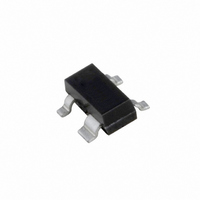
BFG325/XR,215 NXP Semiconductors, BFG325/XR,215 Datasheet - Page 2

BFG325/XR,215
Manufacturer Part Number
BFG325/XR,215
Description
TRANS NPN 6V 35MA 14GHZ SOT143R
Manufacturer
NXP Semiconductors
Datasheet
1.BFG325XR215.pdf
(12 pages)
Specifications of BFG325/XR,215
Package / Case
SOT-143, SOT-143B, TO-253AA
Transistor Type
NPN
Voltage - Collector Emitter Breakdown (max)
6V
Frequency - Transition
14GHz
Noise Figure (db Typ @ F)
1.1dB @ 2GHz
Gain
18.3dB
Power - Max
210mW
Dc Current Gain (hfe) (min) @ Ic, Vce
60 @ 15mA, 3V
Current - Collector (ic) (max)
35mA
Mounting Type
Surface Mount
Dc Collector/base Gain Hfe Min
60
Dc Current Gain Hfe Max
60 @ 15mA @ 3V
Minimum Operating Temperature
- 65 C
Mounting Style
SMD/SMT
Configuration
Dual
Transistor Polarity
NPN
Maximum Operating Frequency
14000 MHz (Typ)
Collector- Emitter Voltage Vceo Max
6 V
Emitter- Base Voltage Vebo
2 V
Continuous Collector Current
35 mA
Power Dissipation
210 mW
Maximum Operating Temperature
+ 175 C
Lead Free Status / RoHS Status
Lead free / RoHS Compliant
Lead Free Status / RoHS Status
Lead free / RoHS Compliant, Lead free / RoHS Compliant
Other names
568-1977-2
934057939215
BFG325/XR T/R
934057939215
BFG325/XR T/R
Philips Semiconductors
2. Pinning information
3. Ordering information
4. Marking
5. Limiting values
9397 750 14247
Product data sheet
Table 1:
[1]
[2]
Table 2:
Table 3:
Table 4:
[1]
Table 5:
In accordance with the Absolute Maximum Rating System (IEC 60134).
Symbol Parameter
NF
Pin
1
2
3
4
Type number
BFG325/XR
Type number
BFG325/XR
Symbol
V
V
V
s
CBO
CEO
EBO
21
2
T
G
* = p: made in Hong Kong.
sp
max
is the temperature at the soldering point of the collector pin.
is the maximum power gain, if K > 1. If K < 1 then G
insertion power gain
noise figure
Parameter
collector-base voltage
collector-emitter voltage
emitter-base voltage
Quick reference data
Pinning
Ordering information
Marking codes
Limiting values
Description
collector
emitter
base
emitter
Package
Name
SC-61AA plastic surface mounted package; reverse pinning;
Rev. 01 — 2 February 2005
Description
4 leads
…continued
Conditions
I
f = 1.8 GHz; T
Z
V
C
S
s
CE
= 15 mA; V
=
= Z
= 3 V; f = 2 GHz
opt
L
= 50
; I
Conditions
open emitter
open base
open collector
C
= 3 mA;
Marking code
S2*
CE
amb
= 3 V;
Simplified outline
= 25 C;
max
= MSG, see
NPN 14 GHz wideband transistor
3
2
© Koninklijke Philips Electronics N.V. 2005. All rights reserved.
[1]
1
4
Min
-
-
Figure
BFG325/XR
4.
Typ
14
1.1
Symbol
Min
-
-
-
3
Max
-
-
Max
15
6
2
sym086
Version
SOT143R
2, 4
1
Unit
dB
dB
Unit
V
V
V
2 of 12


