NE68119-T1-A CEL, NE68119-T1-A Datasheet - Page 2
NE68119-T1-A
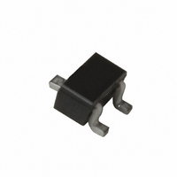
Manufacturer Part Number
NE68119-T1-A
Description
TRANSISTOR NPN 1GHZ SMD
Manufacturer
CEL
Specifications of NE68119-T1-A
Transistor Type
NPN
Voltage - Collector Emitter Breakdown (max)
10V
Frequency - Transition
7GHz
Noise Figure (db Typ @ F)
1.4dB ~ 1.8dB @ 1GHz ~ 2GHz
Gain
10dB ~ 14dB
Power - Max
100mW
Dc Current Gain (hfe) (min) @ Ic, Vce
80 @ 7mA, 3V
Current - Collector (ic) (max)
65mA
Mounting Type
Surface Mount
Package / Case
Surface Mount
Configuration
Single
Transistor Polarity
NPN
Continuous Collector Current
0.065 A
Power Dissipation
0.1 W
Lead Free Status / RoHS Status
Lead free / RoHS Compliant
Other names
2SC5007-T1-A
NE68119-ATR
NE68119-ATR
Available stocks
Company
Part Number
Manufacturer
Quantity
Price
Company:

Part Number:
NE68119-T1-A
Manufacturer:
CEL
Quantity:
12 000
Part Number:
NE68119-T1-A
Manufacturer:
RENESAS/瑞萨
Quantity:
20 000


ELECTRICAL CHARACTERISTICS
ELECTRICAL CHARACTERISTICS
Notes:
1. Electronic Industrial Association of Japan.
2. Pulsed (PW ≤ 350 ms, duty cycle ≤ 2 %).
3. The emitter terminal should be connected to the ground terminal of the 3 terminal capacitance bridge.
SYMBOLS
SYMBOLS
R
|S
R
C
TH (J-A)
|S
I
G
I
h
NF
CBO
EBO
C
TH (J-A)
21E
P
G
I
I
f
RE 3
h
NF
CBO
EBO
FE
NF
21E
P
T
f
RE 3
T
FE
NF
T
T
|
2
|
2
Gain Bandwidth Product at
V
V
Noise Figure at V
Associated Gain at V
Insertion Power Gain at
V
Forward Current Gain
Collector Cutoff Current at
V
Emitter Cutoff Current at
V
Feedback Capacitance at
V
V
Thermal Resistance (Junction to Ambient) °C/W
Total Power Dissipation
Gain Bandwidth Product at V
V
Noise Figure at V
Associated Gain at V
Insertion Power Gain at V
Forward Current Gain
V
Collector Cutoff Current at V
Emitter Cutoff Current at V
Feedback Capacitance at
V
Thermal Resistance (Junction to Ambient)
Total Power Dissipation
V
V
CE
CE
CE
CB
EB
CB
CB
CE
CE
CE
CE
CB
PARAMETERS AND CONDITIONS
= 8 V, I
= 3 V, I
= 8 V, I
= 10 V, I
= 1 V, I
= 3 V, I
= 10 V, I
= 3 V, I
= 3 V, I
= 10 V, I
= 8 V, I
= 3 V, I
PARAMETERS AND CONDITIONS
EIAJ
EIAJ
C
C
C
C
E
C
C
1
PACKAGE OUTLINE
C
C
E
E
PACKAGE OUTLINE
= 0 mA, f = 1 MHz
1
E
= 20 mA
= 7 mA
= 20 mA, f = 1 GHz
= 0 mA
REGISTERED NUMBER
= 7 mA
= 7 mA
= 20 mA
= 7 mA
REGISTERED NUMBER
PART NUMBER
= 0 mA
= 0 mA, f = 1 MHz
= 0 mA, f = 1 MHz
f = 1 GHz
f = 2 GHz
f = 1 GHz
f = 2 GHz
PART NUMBER
CE
CE
= 8 V, I
= 8 V, I
CE
CE
2
2
at
at V
= 8 V, I
= 8 V, I
f = 2 GHz
CE
f = 1 GHz
f = 2 GHz
f = 1 GHz
f = 2 GHz
EB
C
C
CE
CB
= 8 V, I
CE
= 7 mA,
= 7 mA, f = 1 GHz
= 1 V, I
= 8 V, I
(T
(T
C
C
= 10 V, I
= 8 V, I
A
= 7 mA,
A
= 7 mA,
= 25°C)
= 25°C)
C
C
C
= 20 mA,
f = 2 GHz
C
= 20 mA
= 0 mA
E
= 20 mA
= 0 mA
UNITS MIN TYP MAX MIN TYP MAX MIN
GHz
GHz
mW
dB
dB
dB
dB
dB
dB
µA
µA
pF
pF
50
9
00 (CHIP)
NE68100
100
9.0
1.6
0.2
12
17
11
UNITS
°C/W
GHz
GHz
mW
dB
dB
dB
dB
dB
dB
µA
µA
pF
600
250
1.0
1.0
2.3
0.7
80
13
50
MIN TYP MAX MIN
50
NE68118
2SC5012
NE68133
2SC3583
0.25
100
9.0
1.2
18
14
15
0.35
9.0
100
9
1.2
33
13
11
250
833
150
2.5
1.0
1.0
0.8
12.5
250
625
200
1.0
1.0
0.9
2
7
80
50
9
NE68119
2SC5007
NE68135
2SC3604
TYP MAX MIN
0.45
7.0
1.4
1.8
19
14
10
TYP MAX MIN TYP MAX
14
100
8
9.0
1.6
0.2
11
35
12
1000
160
100
1.0
1.0
0.9
250
590
295
2.3
1.0
1.0
0.7
NE681 SERIES
40
50
NE68139/39R
NE68130
2SC4227
2SC4094
TYP MAX
13.5
0.45
7.0
1.5
1.6
7.5
13.5
0.25
30
13
100
9.0
1.2
8.5
9
15
39
240
833
150
1.0
1.0
0.9
200
625
200
1.0
1.0
0.8
2
Related parts for NE68119-T1-A
Image
Part Number
Description
Manufacturer
Datasheet
Request
R

Part Number:
Description:
TRANSISTOR NPN 1GHZ SMD
Manufacturer:
CEL
Datasheet:

Part Number:
Description:
TRANS NPN 1GHZ SMD
Manufacturer:
CEL
Datasheet:

Part Number:
Description:
Dantona CEL-V325-HC Cell Phone Battery Fits Motorola Q & BT-50
Manufacturer:
DANTONA INDUSTRIES
Part Number:
Description:
FRS RADIO BATTERIES 3.6 VOLTS / 1600 MAH
Manufacturer:
DANTONA INDUSTRIES
Part Number:
Description:
LITHIUM ION 900MA FOR USE WITH NOKIA 3360 CELL PHONE
Manufacturer:
DANTONA INDUSTRIES
Part Number:
Description:
CELL PHONE BATTERY FOR MOTOROLA V3 CELLULAR PHONE
Manufacturer:
DANTONA INDUSTRIES
Part Number:
Description:
Transistor Output Optocouplers DISC BY CEL 6/00 SO-6 PHOTOCOUPLER
Manufacturer:
CEL
Datasheet:
Part Number:
Description:
Transistor Output Optocouplers DISC BY CEL 8/00 DIP-6 PHOTO COUPLER
Manufacturer:
CEL
Datasheet:
Part Number:
Description:
Transistor Output Optocouplers DISC BY CEL 11/00 DIP-6 PHOTO COUPLER
Manufacturer:
CEL
Datasheet:
Part Number:
Description:
Transistor Output Optocouplers DISC BY CEL 6/00 DIP-6 PHOTO COUPLER
Manufacturer:
CEL
Datasheet:
Part Number:
Description:
Transistor Output Optocouplers DISC BY CEL 5/00 DIP-6 PHOTO COUPLER
Manufacturer:
CEL
Datasheet: