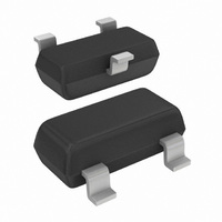
BFT92,215 NXP Semiconductors, BFT92,215 Datasheet - Page 2

BFT92,215
Manufacturer Part Number
BFT92,215
Description
TRANS PNP 25MA 15V 5GHZ SOT23
Manufacturer
NXP Semiconductors
Datasheet
1.BFT92215.pdf
(10 pages)
Specifications of BFT92,215
Package / Case
SOT-23-3, TO-236-3, Micro3™, SSD3, SST3
Transistor Type
PNP
Voltage - Collector Emitter Breakdown (max)
15V
Frequency - Transition
5GHz
Noise Figure (db Typ @ F)
2.5dB @ 500MHz
Power - Max
300mW
Dc Current Gain (hfe) (min) @ Ic, Vce
20 @ 14mA, 10V
Current - Collector (ic) (max)
25mA
Mounting Type
Surface Mount
Dc Collector/base Gain Hfe Min
20 @ 14 mA @ 10 V
Minimum Operating Temperature
- 65 C
Mounting Style
SMD/SMT
Configuration
Single
Transistor Polarity
PNP
Maximum Operating Frequency
5000 MHz (Typ)
Collector- Emitter Voltage Vceo Max
15 V
Emitter- Base Voltage Vebo
2 V
Continuous Collector Current
0.025 A
Power Dissipation
300 mW
Maximum Operating Temperature
+ 175 C
Number Of Elements
1
Collector-emitter Voltage
15V
Collector-base Voltage
20V
Emitter-base Voltage
2V
Collector Current (dc) (max)
25mA
Dc Current Gain (min)
20
Frequency (max)
5GHz
Operating Temp Range
-65C to 175C
Operating Temperature Classification
Military
Mounting
Surface Mount
Pin Count
3
Package Type
TO-236AB
Lead Free Status / RoHS Status
Lead free / RoHS Compliant
Gain
-
Lead Free Status / Rohs Status
Lead free / RoHS Compliant
Other names
568-1655-2
933347730215
BFT92 T/R
933347730215
BFT92 T/R
Available stocks
Company
Part Number
Manufacturer
Quantity
Price
Company:
Part Number:
BFT92,215
Manufacturer:
NXP
Quantity:
36 000
NXP Semiconductors
DESCRIPTION
PNP transistor in a plastic SOT23
envelope.
It is primarily intended for use in RF
wideband amplifiers, such as in aerial
amplifiers, radar systems,
oscilloscopes, spectrum analyzers,
etc. The transistor features low
intermodulation distortion and high
power gain; due to its very high
transition frequency, it also has
excellent wideband properties and
low noise up to high frequencies.
NPN complements are BFR92 and
BFR92A.
QUICK REFERENCE DATA
Note
1. T
November 1992
V
V
I
P
f
C
G
F
d
SYMBOL
C
T
im
CBO
CEO
tot
PNP 5 GHz wideband transistor
re
UM
s
is the temperature at the soldering point of the collector tab.
collector-base voltage
collector-emitter voltage
DC collector current
total power dissipation
transition frequency
feedback capacitance
maximum unilateral power gain
noise figure
intermodulation distortion
PARAMETER
PINNING
PIN
1
2
3
base
emitter
collector
open emitter
open base
up to T
I
I
I
f = 500 MHz; T
I
T
I
V
f
C
C
C
C
C
(pq-r)
Code: W1p
amb
o
= 14 mA; V
= 2 mA; V
= 14 mA; V
= 5 mA; V
= 14 mA; V
= 150 mV; T
DESCRIPTION
= 25 C
= 493.25 MHz
2
s
= 95 C; note 1
CONDITIONS
CE
CE
CE
CE
amb
CE
amb
= 10 V; f = 1 MHz
= 10 V; f = 500 MHz;
= 10 V; f = 500 MHz
= 10 V;
= 10 V; R
= 25 C
= 25 C;
lfpage
L
= 75 ;
Top view
1
Fig.1 SOT23.
5
0.7
18
2.5
60
Product specification
TYP.
3
MSB003
20
15
25
300
MAX.
BFT92
2
V
V
mA
mW
GHz
pF
dB
dB
dB
UNIT


