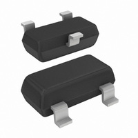
BFS17A,215 NXP Semiconductors, BFS17A,215 Datasheet - Page 3

BFS17A,215
Manufacturer Part Number
BFS17A,215
Description
TRANS NPN 25MA 15V 3GHZ SOT23
Manufacturer
NXP Semiconductors
Datasheet
1.BFS17A215.pdf
(9 pages)
Specifications of BFS17A,215
Package / Case
SOT-23-3, TO-236-3, Micro3™, SSD3, SST3
Transistor Type
NPN
Voltage - Collector Emitter Breakdown (max)
15V
Frequency - Transition
2.8GHz
Noise Figure (db Typ @ F)
2.5dB @ 800MHz
Power - Max
300mW
Dc Current Gain (hfe) (min) @ Ic, Vce
25 @ 2mA, 1V
Current - Collector (ic) (max)
25mA
Mounting Type
Surface Mount
Dc Current Gain Hfe Max
25 @ 2mA @ 1V
Mounting Style
SMD/SMT
Configuration
Single
Transistor Polarity
NPN
Maximum Operating Frequency
2800 MHz (Typ)
Collector- Emitter Voltage Vceo Max
15 V
Emitter- Base Voltage Vebo
2.5 V
Continuous Collector Current
0.025 A
Power Dissipation
300 mW
Maximum Operating Temperature
+ 150 C
Number Of Elements
1
Collector-emitter Voltage
15V
Collector-base Voltage
25V
Emitter-base Voltage
2.5V
Collector Current (dc) (max)
25mA
Dc Current Gain (min)
25
Frequency (max)
2.8GHz
Operating Temp Range
-65C to 150C
Operating Temperature Classification
Military
Mounting
Surface Mount
Pin Count
3
Package Type
TO-236AB
Lead Free Status / RoHS Status
Lead free / RoHS Compliant
Gain
-
Lead Free Status / Rohs Status
Lead free / RoHS Compliant
Other names
568-1653-2
933750250215
BFS17A T/R
933750250215
BFS17A T/R
NXP Semiconductors
THERMAL CHARACTERISTICS
Note
1. T
CHARACTERISTICS
T
Notes
1. G
2. d
September1995
R
I
h
f
C
C
C
G
F
V
SYMBOL
SYMBOL
j
CBO
T
FE
= 25 C unless otherwise specified.
O
NPN 3 GHz wideband transistor
th j-s
c
e
re
UM
V
V
V
measured at f
s
im
p
q
r
UM
= V
is the temperature at the soldering point of the collector pin.
= V
= V
= 60 dB (DIN 45004B); I
is the maximum unilateral power gain, assuming S
O
O
O
; f
6 dB; f
6 dB; f
thermal resistance from junction to soldering point
collector cut-off current
DC current gain
transition frequency
collector capacitance
emitter capacitance
feedback capacitance
maximum unilateral power gain
note 1
noise figure
output voltage
p
= 795.25 MHz;
(p+qr)
r
q
= 805.25 MHz;
PARAMETER
= 803.25 MHz;
= 793.25 MHz.
PARAMETER
C
= 14 mA; V
CE
I
I
I
I
T
I
T
I
I
I
I
f = 800 MHz; T
note 2
E
C
C
C
E
C
C
C
C
amb
amb
= 0; V
= 0; V
= 2 mA; V
= 25 mA; V
= 25 mA; V
= 0; V
= 0; V
= 14 mA; V
= 2 mA; V
= 10 V; R
= 25 C
= 25 C
CB
CB
EB
CE
= 10 V
= 10 V; f = 1 MHz;
= 0.5 V; f = 1 MHz
= 5 V; f = 1 MHz
CONDITIONS
L
3
CE
CE
12
= 75 ; T
CE
CE
CE
amb
is zero and
= 1 V; T
= 5 V; Z
= 1 V; T
= 5 V; f = 500 MHz;
= 10 V; f = 800 MHz
= 25 C
up to T
amb
amb
S
amb
= 60 ;
CONDITIONS
s
= 25 C;
= 25 C
G
= 70 C; note 1
= 25 C
UM
=
10 log
25
25
MIN.
--------------------------------------------------------- -
1
–
90
90
2.8
0.7
1.25
0.6
13.5
2.5
150
S
TYP.
11
VALUE
260
Product specification
S
2
1
21
2
50
–
MAX.
BFS17A
S
22
2
UNIT
K/W
nA
GHz
pF
pF
pF
dB
dB
mV
UNIT
dB.


