MRF9060LR1 Freescale Semiconductor, MRF9060LR1 Datasheet
MRF9060LR1
Specifications of MRF9060LR1
Available stocks


Related parts for MRF9060LR1

MRF9060LR1 Summary of contents
Page 1
... CASE 360B - 05, STYLE 1 CASE 360C - 05, STYLE 1 Symbol V DSS V GS MRF9060LR1 P D MRF9060LSR1 T stg Symbol MRF9060LR1 R θJC MRF9060LSR1 M1 (Minimum) MRF9060LR1 MRF9060LSR1 Rev. 9, 5/2006 BROADBAND NI - 360 MRF9060LR1 NI - 360S MRF9060LSR1 Value Unit - 0.5, +65 Vdc - 0. Vdc 159 W 0.91 W/°C 219 W 1.25 W/° +150 °C 150 ° ...
Page 2
... GS D Forward Transconductance ( Vdc Adc Dynamic Characteristics Input Capacitance ( Vdc ± 30 mV(rms) MHz Output Capacitance ( Vdc ± 30 mV(rms) MHz Reverse Transfer Capacitance ( Vdc ± 30 mV(rms) MHz MRF9060LR1 MRF9060LSR1 2 = 25°C unless otherwise noted) C Symbol I DSS I DSS I GSS V GS(th) V GS(Q) V DS(on iss ...
Page 3
... C Symbol G ps η IMD IRL G ps η IMD IRL P 1dB G ps η Min Typ Max 16 17 — — — — — 17 — — 39 — — — — — — 70 — — 17 — — 51 — MRF9060LR1 MRF9060LSR1 Unit dB % dBc dBc ...
Page 4
... V Tantalum Chip Capacitor C10 3.0 pF Chip Capacitor C12 0.5 pF Chip Capacitor (MRF9060) 0.7 pF Chip Capacitor (MRF9060S) C17 220 mF Electrolytic Chip Capacitor L1, L2 12.5 nH Inductors N1 Type Panel Mount, Stripline WB1, WB2 10 mil Brass Wear Blocks MRF9060LR1 MRF9060LSR1 Z10 Z11 DUT Z10 ...
Page 5
... PCBs may have either Motorola or Freescale markings during the transition period. These changes will have no impact on form, fit or function of the current product. Figure 2. 930 - 960 MHz Broadband Test Circuit Component Layout RF Device Data Freescale Semiconductor B2 C7 C13 WB1 WB2 C10 C17 V DD C15 C16 OUTPUT C14 C11 C12 MRF9060 900 MHz Rev−02 MRF9060LR1 MRF9060LSR1 5 ...
Page 6
... MHz −30 3rd Order −40 −50 5th Order −60 −70 0 OUTPUT POWER (WATTS) PEP out Figure 6. Intermodulation Distortion Products versus Output Power MRF9060LR1 MRF9060LSR1 6 TYPICAL CHARACTERISTICS Vdc (PEP) out I = 450 mA DQ IMD Two−Tone Measurement, 100 kHz Tone Spacing ...
Page 7
... IMD 6 RF Device Data Freescale Semiconductor TYPICAL CHARACTERISTICS Vdc 450 945 MHz f2 = 945.1 MHz OUTPUT POWER (WATTS) PEP out Figure 8. Power Gain, Efficiency, and IMD versus Output Power −20 −40 −60 100 MRF9060LR1 MRF9060LSR1 7 ...
Page 8
... Z Z Figure 9. Series Equivalent Source and Load Impedance MRF9060LR1 MRF9060LSR1 Ω load source f = 960 MHz f = 930 MHz f = 960 MHz f = 930 MHz 450 mA PEP DD DQ out source load MHz Ω Ω 930 0.80 - j0.10 2.08 - j0.65 945 0.80 - j0.05 2.07 - j0.38 960 ...
Page 9
... RF Device Data Freescale Semiconductor NOTES MRF9060LR1 MRF9060LSR1 9 ...
Page 10
... MRF9060LR1 MRF9060LSR1 10 NOTES RF Device Data Freescale Semiconductor ...
Page 11
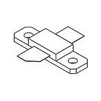
... M 0.355 0.365 9.02 9.27 N 0.357 0.363 9.07 9.22 R 0.227 0.23 5.77 5.92 S 0.225 0.235 5.72 5.97 aaa 0.005 REF 0.13 REF bbb 0.010 REF 0.25 REF ccc 0.015 REF 0.38 REF STYLE 1: PIN 1. DRAIN 2. GATE 3. SOURCE MRF9060LR1 MRF9060LSR1 11 ...
Page 12
... P.O. Box 5405 Denver, Colorado 80217 1 - 800- 441- 2447 or 303 - 675- 2140 Fax: 303 - 675- 2150 LDCForFreescaleSemiconductor@hibbertgroup.com MRF9060LR1 MRF9060LSR1 Document Number: MRF9060 Rev. 9, 5/2006 12 Information in this document is provided solely to enable system and software implementers to use Freescale Semiconductor products. There are no express or implied copyright licenses granted hereunder to design or fabricate any integrated circuits or integrated circuits based on the information in this document ...