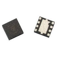
ATF-501P8-TR1 Avago Technologies US Inc., ATF-501P8-TR1 Datasheet - Page 2

ATF-501P8-TR1
Manufacturer Part Number
ATF-501P8-TR1
Description
IC PHEMT 2GHZ 4.5V 280MA 8-LPCC
Manufacturer
Avago Technologies US Inc.
Datasheet
1.ATF-501P8-BLK.pdf
(22 pages)
Specifications of ATF-501P8-TR1
Gain
15dB
Transistor Type
pHEMT FET
Frequency
2GHz
Voltage - Rated
7V
Current Rating
1A
Noise Figure
1dB
Current - Test
280mA
Voltage - Test
4.5V
Power - Output
29dBm
Package / Case
8-LPCC
Drain Source Voltage Vds
4.5V
Continuous Drain Current Id
1A
Power Dissipation Pd
3.5W
Noise Figure Typ
1dB
Rf Transistor Case
LPCC
No. Of Pins
8
Frequency Max
6GHz
Frequency Min
50MHz
Drain Current Idss Max
280mA
Rohs Compliant
Yes
Lead Free Status / RoHS Status
Lead free / RoHS Compliant
Available stocks
Company
Part Number
Manufacturer
Quantity
Price
Company:
Part Number:
ATF-501P8-TR1
Manufacturer:
AVAGO
Quantity:
32 184
Part Number:
ATF-501P8-TR1
Manufacturer:
AVAGO/安华高
Quantity:
20 000
Company:
Part Number:
ATF-501P8-TR1G
Manufacturer:
AVAGO
Quantity:
10 000
ATF-501P8 Absolute Maximum Ratings
I
I
P
P
T
T
θ
Product Consistency Distribution Charts at 2 GHz, 4.5V, 200 mA
Figure 4. Gain.
Notes:
5. Distribution data sample size is 300 samples taken from 3 different wafers and 3 different lots. Future wafers allocated to this product may have
6. Measurements are made on production test board, which represents a trade-off between optimal OIP3, P1dB and VSWR. Circuit losses have
2
Symbol
V
V
V
DS
GS
100
Figure 1. Typical IV curve (Vgs = 0.01V) per step.
CH
diss
in max.
STG
80
60
40
20
ch_b
800
700
600
500
400
300
200
100
DS
GS
GD
0
13
0
nominal values anywhere between the upper and lower limits.
been de-embedded from actual measurements.
0
Cpk=1.61
Stdev=0.33
1
–3 Std
14
2
GAIN (dB)
Parameter
Drain–Source Voltage
Gate–Source Voltage
Gate Drain Voltage
Drain Current
Gate Current
Total Power Dissipation
RF Input Power
Channel Temperature
Storage Temperature
Thermal Resistance
Vds (V)
15
3
Vgs=0.7V
Vgs=0.65V
Vgs=0.6V
Vgs=0.55V
Vgs=0.5V
4
+3 Std
16
[2]
5
[2]
17
[4]
6
[2]
[2]
[3]
[1]
Figure 2. P1dB.
Figure 5. OIP3.
120
100
100
80
60
40
20
80
60
40
20
0
0
27.5
42
Cpk=1.76
Stdev=0.3
Cpk=1.1
Stdev=0.87
Units
V
V
V
A
mA
W
dBm
°C
°C
°C/W
–3 Std
43
28
–3 Std
44
28.5
45
P1dB (dBm)
OIP3 (dBm)
29
46
47
Absolute
Maximum
7
-5 to 0.8
-5 to 1
1
12
3.5
30
150
-65 to 150
23
29.5
+3 Std
[5,6]
+3 Std
48
30
49
30.5
50
Notes:
1. Operation of this device in excess of
2. Assumes DC quiescent conditions.
3. Board (package belly) temperatureT
4. Channel-to-board
Figure 3. PAE.
120
100
80
60
40
20
0
45
any one of these parameters may cause
permanent damage.
25°C. Derate 43.5 mW/°C for T
measured using 150°C Liquid Crystal
Measurement method.
Cpk=1.51
Stdev=3.38
–3 Std
55
PAE (%)
65
thermal
+3 Std
75
B
> 69.5°C.
resistance
85
B
is


