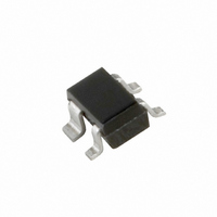
BF1109WR,115 NXP Semiconductors, BF1109WR,115 Datasheet - Page 6

BF1109WR,115
Manufacturer Part Number
BF1109WR,115
Description
MOSFET N-CH 11V 30MA CMPAK-4
Manufacturer
NXP Semiconductors
Datasheet
1.BF1109WR115.pdf
(15 pages)
Specifications of BF1109WR,115
Package / Case
CMPAK-4
Transistor Type
N-Channel Dual Gate
Frequency
800MHz
Gain
20dB
Voltage - Rated
11V
Current Rating
30mA
Noise Figure
1.5dB
Voltage - Test
9V
Configuration
Single Dual Gate
Continuous Drain Current
0.03 A
Drain-source Breakdown Voltage
11 V
Maximum Operating Temperature
+ 150 C
Minimum Operating Temperature
- 65 C
Mounting Style
SMD/SMT
Power Dissipation
200 mW
Transistor Polarity
N-Channel
Lead Free Status / RoHS Status
Lead free / RoHS Compliant
Power - Output
-
Current - Test
-
Lead Free Status / Rohs Status
Lead free / RoHS Compliant
Other names
934050280115
BF1109WR T/R
BF1109WR T/R
BF1109WR T/R
BF1109WR T/R
NXP Semiconductors
1997 Dec 08
handbook, halfpage
handbook, halfpage
N-channel dual-gate MOS-FETs
V
f
unw
V
T
(dBμV)
Fig.11 Unwanted voltage for 1% cross-modulation
DS
Fig.9
V unw
j
G2-S
= 25 C.
(mA)
= 60 MHz; T
120
110
100
= 9 V; V
I D
90
80
16
12
= 4 V.
8
4
0
0
0
as a function of gain reduction;
typical values (see Fig.18).
Drain current as a function of drain-source
voltage; typical values.
G2nom
amb
= 4 V; I
2
= 25 C.
20
Dnom
4
= 12 mA; f
6
w
gain reduction (dB)
40
= 50 MHz;
8
V DS (V)
MDA619
MDA617
60
10
6
handbook, halfpage
V
Fig.10 Drain current as a function of gate 1 current;
DS
(mA)
I D
= 9 V; V
16
12
8
4
0
BF1109; BF1109R; BF1109WR
−8
typical values.
G2-S
= 4 V; T
−6
j
= 25 C.
−4
Product specification
−2
I G1 (μA)
MDA618
0


