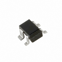
BF904WR,115 NXP Semiconductors, BF904WR,115 Datasheet - Page 7

BF904WR,115
Manufacturer Part Number
BF904WR,115
Description
MOSFET N-CH 7V 30MA SOT343R
Manufacturer
NXP Semiconductors
Datasheet
1.BF904WR115.pdf
(14 pages)
Specifications of BF904WR,115
Package / Case
CMPAK-4
Current Rating
30mA
Frequency
200MHz
Transistor Type
N-Channel Dual Gate
Noise Figure
1dB
Current - Test
10mA
Voltage - Test
5V
Configuration
Dual Common Source
Transistor Polarity
N-Channel
Drain-source Breakdown Voltage
7 V
Gate-source Breakdown Voltage
6 V
Continuous Drain Current
0.03 A
Power Dissipation
280 mW
Maximum Operating Temperature
+ 150 C
Mounting Style
SMD/SMT
Minimum Operating Temperature
- 65 C
Lead Free Status / RoHS Status
Lead free / RoHS Compliant
Power - Output
-
Gain
-
Lead Free Status / RoHS Status
Lead free / RoHS Compliant, Lead free / RoHS Compliant
Other names
934031480115::BF904WR T/R::BF904WR T/R
NXP Semiconductors
2010 Sep 15
handbook, halfpage
handbook, halfpage
N-channel dual-gate MOS-FET
V
R
V
R
Fig.13 Drain current as a function of gate 2 voltage;
(mA)
DS
DS
G1
G
(mA)
I D
I D
= 120 k (connected to V
= 5 V; V
= 120 k (connected to V
Fig.11 Drain current as a function of gate 1
= 5 V; T
12
12
8
4
0
8
4
0
0
0
typical values; see Fig.19.
G2-S
j
= 25 C.
supply voltage (= V
see Fig.19.
= 4 V.
1
2
GG
2
GG
).
); T
j
= 25 C.
3
GG
4
); typical values;
V
GG
V
G2 S
4
V
= 5 V
GG
4.5 V
4 V
3.5 V
3 V
MLD275
MLD276
(V)
(V)
6
5
7
handbook, halfpage
handbook, halfpage
V
R
V
R
G2-S
DS
G1
G
(mA)
(μA)
I G1
I D
= 120 k (connected to V
connected to V
= 5 V; T
Fig.14 Gate 1 current as a function of gate 2
20
15
10
= 4 V.
Fig.12 Drain current as a function of gate 1
40
30
20
10
5
0
0
0
0
j
= 25 C.
voltage; typical values; see Fig.19.
(= V
typical values; see Fig.19.
GG
2
GG
; T
j
) and drain supply voltage;
R
= 25 C.
2
G1
GG
= 47 kΩ
).
4
V
GG
68 kΩ
4
Product specification
V
= V
V
6
GG
G2 S
BF904WR
DS
= 5 V
100 kΩ
120 kΩ
150 kΩ
180 kΩ
220 kΩ
(V)
4.5 V
4 V
3.5 V
3 V
MLD274
82 kΩ
MLB945
(V)
8
6


