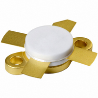
BLF147,112 NXP Semiconductors, BLF147,112 Datasheet - Page 6

BLF147,112
Manufacturer Part Number
BLF147,112
Description
TRANSISTOR RF DMOS SOT121B
Manufacturer
NXP Semiconductors
Datasheet
1.BLF147112.pdf
(15 pages)
Specifications of BLF147,112
Package / Case
SOT-121B
Transistor Type
N-Channel
Frequency
108MHz
Gain
14dB
Voltage - Rated
65V
Current Rating
25A
Voltage - Test
28V
Power - Output
150W
Minimum Operating Temperature
- 65 C
Mounting Style
SMD/SMT
Resistance Drain-source Rds (on)
0.15 Ohm @ 10 V
Transistor Polarity
N-Channel
Configuration
Single Dual Source
Drain-source Breakdown Voltage
65 V
Gate-source Breakdown Voltage
+/- 20 V
Continuous Drain Current
25 A
Power Dissipation
220000 mW
Maximum Operating Temperature
+ 200 C
Application
HF/VHF
Channel Type
N
Channel Mode
Enhancement
Drain Source Voltage (max)
65V
Output Power (max)
150W
Power Gain (typ)@vds
19@28VdB
Frequency (max)
108MHz
Package Type
CRFM
Pin Count
4
Forward Transconductance (typ)
7.5S
Drain Source Resistance (max)
150@10Vmohm
Input Capacitance (typ)@vds
450@28VpF
Output Capacitance (typ)@vds
360@28VpF
Reverse Capacitance (typ)
55@28VpF
Operating Temp Range
-65C to 200C
Drain Efficiency (typ)
40%
Mounting
Screw
Mode Of Operation
SSB Class-AB
Number Of Elements
1
Power Dissipation (max)
220000mW
Vswr (max)
50
Screening Level
Military
Lead Free Status / RoHS Status
Lead free / RoHS Compliant
Noise Figure
-
Current - Test
-
Lead Free Status / Rohs Status
Lead free / RoHS Compliant
Other names
568-2385
933930000112
BLF147
BLF147
933930000112
BLF147
BLF147
NXP Semiconductors
APPLICATION INFORMATION FOR CLASS-AB OPERATION
RF performance in SSB operation in a common source class-AB circuit.
T
Notes
1. Optimum load impedance: 2.1 + j0 .
2. Maximum values at drive levels within the specified PEP values for either amplified tone. For the peak envelope
Ruggedness in class-AB operation
The BLF147 is capable of withstanding a load mismatch corresponding to VSWR = 50:1 through all phases under the
following conditions: V
handbook, halfpage
20 to 150 (PEP)
h
VHF power MOS transistor
= 25 C; R
V
Fig.8
power the values should be decreased by 6 dB.
(pF)
GS
C rs
500
400
300
200
100
= 0; f = 1 MHz.
0
(W)
P
0
L
Feedback capacitance as a function of
drain-source voltage; typical values.
th mb-h
10
= 0.2 K/W; R
DS
(MHz)
= 28 V; f = 28 MHz at rated load power.
28
f
20
GS
= 9.8
30
V
V DS (V)
(V)
28
DS
MRA902
f
1
= 28.000 MHz; f
40
Rev. 06 - 5 December 2006
I
(A)
DQ
1
2
= 28.001 MHz; unless otherwise specified.
typ. 19
(dB)
G
17
p
typ. 40
(%)
35
D
(note 2)
typ. 34
(dB)
d
Product specification
30
3
BLF147
6 of 15
(note 2)
typ. 40
(dB)
d
30
5


