BLF542,112 NXP Semiconductors, BLF542,112 Datasheet - Page 5
BLF542,112
Manufacturer Part Number
BLF542,112
Description
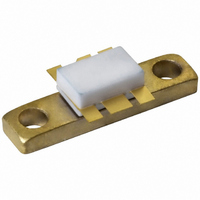
TRANSISTOR RF DMOS SOT171A
Manufacturer
NXP Semiconductors
Datasheet
1.BLF542112.pdf
(15 pages)
Specifications of BLF542,112
Package / Case
SOT-171A
Transistor Type
N-Channel
Frequency
500MHz
Gain
16.5dB
Voltage - Rated
65V
Current Rating
1.5A
Current - Test
50mA
Voltage - Test
28V
Power - Output
5W
Minimum Operating Temperature
- 65 C
Mounting Style
SMD/SMT
Product Type
RF MOSFET Power
Resistance Drain-source Rds (on)
5 Ohms
Transistor Polarity
N-Channel
Configuration
Single Quad Source
Drain-source Breakdown Voltage
65 V
Gate-source Breakdown Voltage
+/- 20 V
Continuous Drain Current
1.5 A
Power Dissipation
20 W
Maximum Operating Temperature
+ 200 C
Application
UHF
Channel Type
N
Channel Mode
Enhancement
Drain Source Voltage (max)
65V
Output Power (max)
5W
Power Gain (typ)@vds
16.5@28VdB
Frequency (max)
500MHz
Package Type
CDFM
Pin Count
6
Forward Transconductance (typ)
0.24S
Drain Source Resistance (max)
5000@15Vmohm
Input Capacitance (typ)@vds
14@28VpF
Output Capacitance (typ)@vds
9.4@28VpF
Reverse Capacitance (typ)
1.7@28VpF
Operating Temp Range
-65C to 200C
Drain Efficiency (typ)
59%
Mounting
Screw
Mode Of Operation
CW Class-B
Number Of Elements
1
Power Dissipation (max)
20000mW
Vswr (max)
50
Screening Level
Military
Lead Free Status / RoHS Status
Lead free / RoHS Compliant
Noise Figure
-
Lead Free Status / Rohs Status
Compliant
Other names
568-2417
934006660112
BLF542
BLF542
934006660112
BLF542
BLF542
Available stocks
Company
Part Number
Manufacturer
Quantity
Price
Company:

Part Number:
BLF542,112
Manufacturer:
Skyworks
Quantity:
1 400


Philips Semiconductors
2003 Sep 18
handbook, halfpage
handbook, halfpage
R DS (on)
UHF power MOS transistor
V
Fig.4
I
Fig.6
D
(mV/K)
DS
( )
T.C.
= 0.3 A; V
= 10 V.
–2
–4
4
2
0
6
4
2
0
0
0
Temperature coefficient of gate-source
voltage as a function of drain current; typical
values.
Drain-source on-resistance as a function of
junction temperature; typical values.
GS
= 15 V
100
50
200
100
I D (mA)
T j (
o
MBB777
C)
MBB778
300
150
5
handbook, halfpage
handbook, halfpage
V
Fig.5
V
Fig.7
DS
GS
(pF)
1.5
(A)
0.5
= 10 V; T
C
= 0; f = 1 MHz.
I D
30
20
10
1
0
0
0
0
Drain current as a function of gate-source
voltage; typical values.
Input and output capacitance as functions
of drain-source voltage; typical values.
j
= 25 C.
10
5
C os
C is
10
20
Product specification
V GS (V)
V DS (V)
BLF542
MBB759
MBB776
15
30
Related parts for BLF542,112
Image
Part Number
Description
Manufacturer
Datasheet
Request
R

Part Number:
Description:
N-channel enhancement mode vertical D-MOS power transistor encapsulated in a 6-lead, SOT171A flange package with a ceramic cap
Manufacturer:
NXP Semiconductors
Datasheet:

Part Number:
Description:
NXP Semiconductors designed the LPC2420/2460 microcontroller around a 16-bit/32-bitARM7TDMI-S CPU core with real-time debug interfaces that include both JTAG andembedded trace
Manufacturer:
NXP Semiconductors
Datasheet:

Part Number:
Description:
NXP Semiconductors designed the LPC2458 microcontroller around a 16-bit/32-bitARM7TDMI-S CPU core with real-time debug interfaces that include both JTAG andembedded trace
Manufacturer:
NXP Semiconductors
Datasheet:
Part Number:
Description:
NXP Semiconductors designed the LPC2468 microcontroller around a 16-bit/32-bitARM7TDMI-S CPU core with real-time debug interfaces that include both JTAG andembedded trace
Manufacturer:
NXP Semiconductors
Datasheet:
Part Number:
Description:
NXP Semiconductors designed the LPC2470 microcontroller, powered by theARM7TDMI-S core, to be a highly integrated microcontroller for a wide range ofapplications that require advanced communications and high quality graphic displays
Manufacturer:
NXP Semiconductors
Datasheet:
Part Number:
Description:
NXP Semiconductors designed the LPC2478 microcontroller, powered by theARM7TDMI-S core, to be a highly integrated microcontroller for a wide range ofapplications that require advanced communications and high quality graphic displays
Manufacturer:
NXP Semiconductors
Datasheet:
Part Number:
Description:
The Philips Semiconductors XA (eXtended Architecture) family of 16-bit single-chip microcontrollers is powerful enough to easily handle the requirements of high performance embedded applications, yet inexpensive enough to compete in the market for hi
Manufacturer:
NXP Semiconductors
Datasheet:
Part Number:
Description:
The XA-S3 device is a member of Philips Semiconductors? XA(eXtended Architecture) family of high performance 16-bitsingle-chip microcontrollers
Manufacturer:
NXP Semiconductors
Datasheet:

Part Number:
Description:
The NXP BlueStreak LH75401/LH75411 family consists of two low-cost 16/32-bit System-on-Chip (SoC) devices
Manufacturer:
NXP Semiconductors
Datasheet:
Part Number:
Description:
The NXP LPC3130/3131 combine an 180 MHz ARM926EJ-S CPU core, high-speed USB2
Manufacturer:
NXP Semiconductors
Datasheet:
Part Number:
Description:
The NXP LPC3141 combine a 270 MHz ARM926EJ-S CPU core, High-speed USB 2
Manufacturer:
NXP Semiconductors
Part Number:
Description:
The NXP LPC3143 combine a 270 MHz ARM926EJ-S CPU core, High-speed USB 2
Manufacturer:
NXP Semiconductors

Part Number:
Description:
The NXP LPC3152 combines an 180 MHz ARM926EJ-S CPU core, High-speed USB 2
Manufacturer:
NXP Semiconductors
Part Number:
Description:
The NXP LPC3154 combines an 180 MHz ARM926EJ-S CPU core, High-speed USB 2
Manufacturer:
NXP Semiconductors