DF02S-E3/77 Vishay, DF02S-E3/77 Datasheet - Page 2
DF02S-E3/77
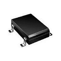
Manufacturer Part Number
DF02S-E3/77
Description
Diode Rectifier Bridge Single 200V 1A 4-Pin Case DFS T/R
Manufacturer
Vishay
Datasheet
1.DF005S-E345.pdf
(4 pages)
Specifications of DF02S-E3/77
Package
4Case DFS
Peak Average Forward Current
1@Ta=40C A
Peak Forward Voltage
1.1 V
Peak Reverse Current
5 uA
Peak Reverse Repetitive Voltage
200 V
Bridge Type
Single Phase
Configuration
Single
Voltage - Peak Reverse (max)
200V
Current - Dc Forward (if)
1A
Diode Type
Single Phase
Speed
Standard Recovery >500ns, > 200mA (Io)
Mounting Type
Surface Mount
Package / Case
4-SMD (DFS)
Product
Single Phase Bridge
Peak Reverse Voltage
200 V
Maximum Rms Reverse Voltage
140 V
Max Surge Current
50 A
Forward Voltage Drop
1.1 V
Maximum Reverse Leakage Current
5 uA
Maximum Operating Temperature
+ 150 C
Length
8.51 mm
Width
6.5 mm
Height
3.3 mm
Mounting Style
SMD/SMT
Minimum Operating Temperature
- 55 C
Phase Type
Single Phase
Number Of Elements
1
Peak Rep Rev Volt
200V
Rms Voltage (max)
140V
Peak Non-repetitive Surge Current (max)
50A
Avg. Forward Curr (max)
1@Ta=40CA
Rev Curr
5uA
Forward Voltage
1.1V
Package Type
Case DFS
Operating Temp Range
-55C to 150C
Pin Count
4
Mounting
Surface Mount
Operating Temperature Classification
Military
Lead Free Status / RoHS Status
Lead free / RoHS Compliant
Reverse Recovery Time (trr)
-
Lead Free Status / Rohs Status
Compliant
Other names
Q3069618
Available stocks
Company
Part Number
Manufacturer
Quantity
Price

Part Number:
DF02S-E3/77
Manufacturer:
VISHAY/威世
Quantity:
20 000


DF005S thru DF10S
Vishay General Semiconductor
Note:
(1) Measured at 1.0 MHz and applied reverse voltage of 4.0 V
Note:
(1) Units mounted on P.C.B. with 0.51 x 0.51" (13 x 13 mm) copper pads
RATINGS AND CHARACTERISTICS CURVES
(T
www.vishay.com
2
ELECTRICAL CHARACTERISTICS (T
PARAMETER
Maximum instantaneous
forward voltage drop per diode
Maximum DC reverse
current at rated DC blocking
voltage per diode
Typical junction
capacitance per diode
THERMAL CHARACTERISTICS (T
PARAMETER
Typical thermal resistance
ORDERING INFORMATION (Example)
PREFERRED P/N
DF06S-E3/45
DF06S-E3/77
A
= 25 °C unless otherwise noted)
1.0
0.5
0
Figure 1. Derating Curve Output Rectified Current
20
P.C.B. Mounted on
0.51 x 0.51" (13 x 13 mm)
Copper Pads
40
Ambient Temperature (°C)
60
(1)
UNIT WEIGHT (g)
(1)
80
PDD-Americas@vishay.com, PDD-Asia@vishay.com, PDD-Europe@vishay.com
0.399
0.399
For technical questions within your region, please contact one of the following:
TEST CONDITIONS SYMBOL DF005S DF01S
1.0 A
T
T
100
A
A
= 25 °C
= 125 °C
120
60 Hz
Resistive or
Inductive Load
PREFERRED PACKAGE CODE
140
A
= 25 °C unless otherwise noted)
160
A
SYMBOL DF005S DF01S
= 25 °C unless otherwise noted)
R
R
V
C
I
θJA
θJL
R
F
J
45
77
Figure 2. Maximum Non-Repetitive Peak Forward Surge
60
50
40
30
20
10
0
BASE QUANTITY
1
DF02S
DF02S
1500
50
Number of Cycles at 60 Hz
DF04S
DF04S
500
1.1
5.0
25
40
15
Current Per Diode
1.0 Cycle
DF06S
DF06S
10
13" diameter paper tape and reel
DELIVERY MODE
T
Single Sine-Wave
Document Number: 88573
J
DF08S
DF08S
= 150 °C
Tube
Revision: 30-Jan-08
DF10S
DF10S
100
UNIT
UNIT
°C/W
µA
pF
V
Related parts for DF02S-E3/77
Image
Part Number
Description
Manufacturer
Datasheet
Request
R

Part Number:
Description:
RECT BRIDGE 1-PHA 200V 1A D-71
Manufacturer:
Vishay
Datasheet:

Part Number:
Description:
RECTIFIER BRIDGE 1AMP 200V DFS
Manufacturer:
Vishay
Datasheet:

Part Number:
Description:
RECTIFIER BRIDGE 1AMP 200V DFS
Manufacturer:
Vishay
Datasheet:
Part Number:
Description:
BRIDGE RECTIFIER,1-PHASE FULL-WAVE,200V V(RRM),SO
Manufacturer:
Vishay
Datasheet:


Part Number:
Description:
DIODE RECTIFIER BRIDGE SINGLE 200V 1A 4DIL
Manufacturer:
Sensitron Semiconductor
Part Number:
Description:
357-036-542-201 CARDEDGE 36POS DL .156 BLK LOPRO
Manufacturer:
Vishay
Datasheet:
Part Number:
Description:
357-036-542-201 CARDEDGE 36POS DL .156 BLK LOPRO
Manufacturer:
Vishay
Datasheet:
Part Number:
Description:
357-036-542-201 CARDEDGE 36POS DL .156 BLK LOPRO
Manufacturer:
Vishay
Datasheet:
Part Number:
Description:
357-036-542-201 CARDEDGE 36POS DL .156 BLK LOPRO
Manufacturer:
Vishay
Datasheet:
Part Number:
Description:
357-036-542-201 CARDEDGE 36POS DL .156 BLK LOPRO
Manufacturer:
Vishay
Datasheet:
Part Number:
Description:
357-036-542-201 CARDEDGE 36POS DL .156 BLK LOPRO
Manufacturer:
Vishay
Datasheet:
Part Number:
Description:
357-036-542-201 CARDEDGE 36POS DL .156 BLK LOPRO
Manufacturer:
Vishay
Datasheet: