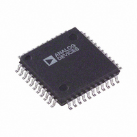
AD6600ASTZ Analog Devices Inc, AD6600ASTZ Datasheet - Page 18

AD6600ASTZ
Manufacturer Part Number
AD6600ASTZ
Description
ADC Single 20MSPS 11-Bit Parallel 44-Pin LQFP
Manufacturer
Analog Devices Inc
Datasheet
1.AD6600ASTZ-REEL.pdf
(24 pages)
Specifications of AD6600ASTZ
Package
44LQFP
Resolution
11 Bit
Sampling Rate
20000 KSPS
Number Of Adcs
1
Number Of Analog Inputs
2
Digital Interface Type
Parallel
Input Type
Voltage
Signal To Noise Ratio
59(Typ) dB
Sample And Hold
Yes
Polarity Of Input Voltage
Bipolar
Number Of Bits
11
Sampling Rate (per Second)
20M
Data Interface
Parallel
Number Of Converters
1
Power Dissipation (max)
976mW
Voltage Supply Source
Single Supply
Operating Temperature
-40°C ~ 85°C
Mounting Type
Surface Mount
Package / Case
44-LQFP
Lead Free Status / RoHS Status
Lead free / RoHS Compliant
Available stocks
Company
Part Number
Manufacturer
Quantity
Price
Company:
Part Number:
AD6600ASTZ
Manufacturer:
Analog Devices Inc
Quantity:
10 000
Part Number:
AD6600ASTZ
Manufacturer:
ADI/亚德诺
Quantity:
20 000
Company:
Part Number:
AD6600ASTZ-REEL
Manufacturer:
Analog Devices Inc
Quantity:
10 000
AD6600
If a low jitter ECL/PECL clock is available, another option is to
ac-couple a differential ECL/PECL signal to the encode input
pins as shown in Figure 19.
Driving the Analog Inputs
As with most new high-speed, high dynamic range analog-to-digital
converters, the analog input to the AD6600 is differential. Differ-
ential inputs allow much improvement in performance on-chip
as IF signals are processed through attenuation and gain stages.
Most of the improvement is a result of differential analog stages
having high rejection of even-order harmonics. There are also
benefits at the PCB level. First, differential inputs have high
common-mode rejection to stray signals such as ground and
power noise. They also provide good rejection to common-mode
signals such as local oscillator feedthrough.
Driving a differential analog input introduces some new chal-
lenges. Most RF/IF amplifiers are single-ended and may not
obviously interface to the AD6600. However, using simple
techniques, a clean interface is possible. The recommended
method to drive the analog input port is shown in Figure 20.
The AD6600 input is actually designed to match easily to a
SAW filter such as SAWTEK 855297. This allows the SAW
filter to be used in a differential mode, which often improves the
operations of a SAW filter. Using network analyzer data for
both the SAW filter output and the AD6600 input ports (see
data tables for AD6600 S
used for maximum power transfer. Often an adequate match
can be achieved simply by using a shunt inductor to make the
port look real (Figure 20). For more details on how to exactly
match networks, see RF Circuit Design by Chris Bowick, ISBN:
0-672-21868-2.
Where gain is required, the AD6630 differential, low noise, IF
gain block is recommended. This amplifier provides 24 dB of
gain and provides limiting to prevent damage to the SAW filter
and AD6600. The AD6630 is designed to reside between two
SAW filters. This low noise device is ideally suited to many
applications of the AD6600. For more information on the
AD6630, reference the AD6630 data sheet.
OUTPUT
MIXER
FROM
PECL
ECL/
SAW #1
11
VT
VT
AD6630
data), a conjugate match can be
0.1 F
0.1 F
ENCODE
ENCODE
SAW #2
AD6600
AD6600
ADC
When general purpose gain blocks are used, matching can easily
be achieved using a transformer. Most gain blocks are available
with 50 Ω input and output ports. Thus matching to the 200 Ω
impedance of the AD6600 requires only a 1:4 (impedance ratio)
transformer as shown in Figure 21.
In the rare case that better matching is required, a conjugate
match between the amplifier selected and the transformer-
coupled analog input can be achieved by placing the matching
network between the amplifier and the transformer (Figure 22).
For more details on matching, see the reference mentioned
previously for more details.
Understanding the External Analog Filter
Two primary trade-offs must be made when designing the exter-
nal resonant filter. The obvious one is the bandwidth of the
filter. The second, not so obvious, trade-off is settling time of
the filter nodes.
Resonant Filter Bandwidth determines the amount of noise that
is limited at the center frequency chosen. If the resonant filter is
too wide, little noise improvement is seen. If the resonant filter
is too narrow, amplitude variation can be seen due to the toler-
ance of filter components. If the narrow filter is off center due to
these tolerances (or drift), the 4×/8× signal will fall on the transi-
tion band of the filter. An optimum starting point for this filter
is approximately 50 MHz.
Resonant Filter Settling limits the amount of capacitance of this
filter. The output of the 4×/8× amplifier is clamped when the
ADC is processing its input (encode high time). This prevents the
amp output from feeding through to the ADC (T/H) and cor-
rupting the ADC results. But, upon the falling edge of encode,
the amp must now come out of clamp and present an accurate
signal to the ADC T/H. The RC of the external filter deter-
mines the settling of the amp. If the amp output does not settle,
the ADC sees an attenuated signal. So obviously, a narrow
bandwidth is desired to improve noise performance; but if the
filter is too narrow, the amp will not settle and the ADC will see
an attenuated signal.
Figure 23 shows a simplified model of the 4×/8× amplifier. A
key point to note is that the resistor values in the collector legs
are 315 Ω nominal with a tolerance of ± 20%. The filter perfor-
mance is determined by these values in conjunction with the
internal parasitic capacitance, board parasitics and the external
filter components.
OUTPUT
MIXER
FROM
OUTPUT
MIXER
FROM
50
BLOCK
GAIN
50
BLOCK
GAIN
MATCHING
NETWORK
AD6600
ADC
AD6600
ADC


