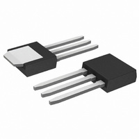
NTD4815NH-1G ON Semiconductor, NTD4815NH-1G Datasheet - Page 4

NTD4815NH-1G
Manufacturer Part Number
NTD4815NH-1G
Description
MOSFET N-CH 30V 6.9A IPAK
Manufacturer
ON Semiconductor
Datasheet
1.NTD4815NH-1G.pdf
(8 pages)
Specifications of NTD4815NH-1G
Fet Type
MOSFET N-Channel, Metal Oxide
Fet Feature
Logic Level Gate
Rds On (max) @ Id, Vgs
15 mOhm @ 30A, 10V
Drain To Source Voltage (vdss)
30V
Current - Continuous Drain (id) @ 25° C
6.9A
Vgs(th) (max) @ Id
2.5V @ 250µA
Gate Charge (qg) @ Vgs
6.8nC @ 4.5V
Input Capacitance (ciss) @ Vds
845pF @ 12V
Power - Max
1.26W
Mounting Type
Through Hole
Package / Case
IPak, TO-251, DPak, VPak (3 straight leads + tab)
Lead Free Status / RoHS Status
Lead free / RoHS Compliant
0.04
0.03
0.02
0.01
80
70
60
50
40
30
20
10
1.8
1.6
1.4
1.2
1.0
0.8
0.6
0
0
--50
0
2
I
V
Figure 3. On- -Resistance vs. Gate- -to- -Source
D
GS
--25
V
3
= 30 A
V
DS
Figure 1. On- -Region Characteristics
Figure 5. On- -Resistance Variation with
GS
= 10 V
, DRAIN--TO--SOURCE VOLTAGE (VOLTS)
, GATE--TO--SOURCE VOLTAGE (VOLTS)
2
4
T
J
10 V
0
, JUNCTION TEMPERATURE (°C)
8 V
6 V
5
25
4
Temperature
6
50
Voltage
7
75
6
8
TYPICAL PERFORMANCE CURVES
100
9
125
10
8
I
T
T
D
J
J
= 30 A
= 25°C
= 25°C
http://onsemi.com
150
3.8 V
4.5 V
4.2 V
11
3.5 V
3.2 V
5 V
4 V
10
12
175
4
10,000
1000
0.05
0.04
0.03
0.02
0.01
100
60
50
40
30
20
10
0
0
10
0
0
Figure 4. On- -Resistance vs. Drain Current and
V
V
Figure 6. Drain- -to- -Source Leakage Current
T
GS
DS
J
V
= 25°C
V
= 0 V
20
DS
≥ 10 V
GS
5
1
Figure 2. Transfer Characteristics
, DRAIN--TO--SOURCE VOLTAGE (VOLTS)
, GATE--TO--SOURCE VOLTAGE (VOLTS)
I
D
30
T
, DRAIN CURRENT (AMPS)
J
10
= 25°C
2
vs. Drain Voltage
T
J
Gate Voltage
= 125°C
T
T
40
J
J
V
= 150°C
= 100°C
V
GS
15
GS
3
= 4.5 V
= 11.5 V
50
T
J
= --55°C
20
4
60
25
5
70
80
30
6


