NTD20N06-001 ON Semiconductor, NTD20N06-001 Datasheet

MOSFET N-CH 60V 20A TO-251A

NTD20N06-001

Manufacturer Part Number
NTD20N06-001
Description
MOSFET N-CH 60V 20A TO-251A
Manufacturer
ON Semiconductor
Datasheet

Specifications of NTD20N06-001

Fet Type
MOSFET N-Channel, Metal Oxide
Fet Feature
Standard
Rds On (max) @ Id, Vgs
46 mOhm @ 10A, 10V
Drain To Source Voltage (vdss)
60V
Current - Continuous Drain (id) @ 25° C
20A
Vgs(th) (max) @ Id
4V @ 250µA
Gate Charge (qg) @ Vgs
30nC @ 10V
Input Capacitance (ciss) @ Vds
1015pF @ 25V
Power - Max
1.36W
Mounting Type
Surface Mount
Package / Case
IPak, TO-251, DPak, VPak (3 straight leads + tab)
Lead Free Status / RoHS Status
Contains lead / RoHS non-compliant
Other names
NTD20N06-001OS
NTD20N06
Power MOSFET
20 Amps, 60 Volts, N−Channel DPAK
supplies, converters and power motor controls and bridge circuits.
Features
Typical Applications
Stresses exceeding Maximum Ratings may damage the device. Maximum
Ratings are stress ratings only. Functional operation above the Recommended
Operating Conditions is not implied. Extended exposure to stresses above the
Recommended Operating Conditions may affect device reliability.
1. When surface mounted to an FR4 board using the minimum recommended
2. When surface mounted to an FR4 board using the 0.5 sq in drain pad size.
MAXIMUM RATINGS
© Semiconductor Components Industries, LLC, 2010
October, 2010 − Rev. 7
Drain−to−Source Voltage
Drain−to−Gate Voltage (R
Gate−to−Source Voltage
Drain Current
Total Power Dissipation @ T
Operating and Storage Temperature Range
Single Pulse Drain−to−Source Avalanche
Thermal Resistance
Maximum Lead Temperature for Soldering
Designed for low voltage, high speed switching applications in power
Lower R
Lower V
Lower Capacitances
Lower Total Gate Charge
Lower and Tighter V
Lower Diode Reverse Recovery Time
Lower Reverse Recovery Stored Charge
These Devices are Pb−Free and are RoHS Compliant
Power Supplies
Converters
Power Motor Controls
Bridge Circuits
pad size.
Derate above 25°C
Energy − Starting T
(V
L = 1.0 mH, I
− Junction−to−Case
− Junction−to−Ambient (Note 1)
− Junction−to−Ambient (Note 2)
Purposes, 1/8″ from case for 10 seconds
DD
− Continuous
− Non−repetitive (t
− Continuous @ T
− Continuous @ T
− Single Pulse (t
= 25 Vdc, V
DS(on)
DS(on)
L
(pk) = 18.4 A, V
Rating
GS
J
p
= 10 Vdc,
(T
= 25°C
v10 ms)
p
A
A
SD
v10 ms)
J
GS
= 25°C
= 100°C
= 25°C unless otherwise noted)
A
A
A
= 10 MW)
= 25°C
= 25°C (Note 1)
= 25°C (Note 2)
DS
= 60 Vdc)
Symbol
T
V
V
R
R
R
J
V
V
E
I
P
DGR
, T
T
DSS
DM
I
I
qJC
qJA
qJA
GS
GS
D
D
AS
D
L
stg
−55 to
Value
"20
"30
0.40
1.88
1.36
175
170
260
110
2.5
60
60
20
10
60
60
80
1
W/°C
°C/W
Unit
Vdc
Vdc
Vdc
Adc
Apk
mJ
°C
°C
W
W
W
See detailed ordering and shipping information in the package
dimensions section on page 2 of this data sheet.
1 2
V
(BR)DSS
60 V
3
ORDERING INFORMATION
4
G
20N06 = Device Code
Y
WW
G
http://onsemi.com
CASE 369C
R
STYLE 2
N−Channel
DPAK
DS(on)
37.5 mW
= Year
= Work Week
= Pb−Free Package
D
Publication Order Number:
TYP
S
Gate
MARKING
DIAGRAM
1
Drain
Drain
NTD20N06/D
4
2
I
D
20 A
MAX
3
Source

Related parts for NTD20N06-001

NTD20N06-001 Summary of contents

Page 1

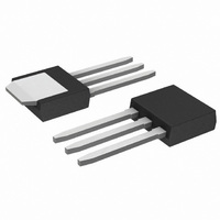
... R 2.5 qJC R 80 qJA R 110 qJA T 260 ° http://onsemi.com R TYP I MAX DS(on N−Channel MARKING DIAGRAM 4 Drain 4 DPAK CASE 369C STYLE Drain Gate Source 20N06 = Device Code Y = Year WW = Work Week G = Pb−Free Package ORDERING INFORMATION Publication Order Number: NTD20N06/D ...

Page 2

... Pulse Test: Pulse Width ≤ 300 ms, Duty Cycle ≤ 2%. 4. Switching characteristics are independent of operating junction temperatures. ORDERING INFORMATION Device NTD20N06G NTD20N06T4G †For information on tape and reel specifications, including part orientation and tape sizes, please refer to our Tape and Reel Packaging Specifications Brochure, BRD8011/ 25°C unless otherwise noted) ...

Page 3

DRAIN−TO−SOURCE VOLTAGE (VOLTS) DS Figure 1. On−Region Characteristics 0.065 0.055 T = ...

Page 4

Switching behavior is most easily modeled and predicted by recognizing that the power MOSFET is charge controlled. The lengths of various switching intervals (Dt) are determined by how fast the FET input capacitance can be charged by current from the ...

Page 5

TOTAL GATE CHARGE (nC) G Figure 8. Gate−To−Source and Drain−To−Source Voltage versus Total Charge DRAIN−TO−SOURCE DIODE CHARACTERISTICS ...

Page 6

SINGLE PULSE T = 25° 100 LIMIT DS(on) THERMAL LIMIT PACKAGE LIMIT 0.1 0 DRAIN−TO−SOURCE VOLTAGE (VOLTS) DS Figure 11. Maximum Rated Forward Biased ...

Page 7

... Z 0.155 −−− 3.93 −−− STYLE 2: PIN 1. GATE 2. DRAIN 3. SOURCE 4. DRAIN 6.172 0.243 mm inches ON Semiconductor Website: www.onsemi.com Order Literature: http://www.onsemi.com/orderlit For additional information, please contact your local Sales Representative NTD20N06/D ...

Related keywords