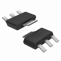
NTF3055-160T3LF ON Semiconductor, NTF3055-160T3LF Datasheet - Page 2

NTF3055-160T3LF
Manufacturer Part Number
NTF3055-160T3LF
Description
MOSFET N-CH 60V 2A SOT223
Manufacturer
ON Semiconductor
Datasheet
1.NTF3055-160T3LF.pdf
(8 pages)
Specifications of NTF3055-160T3LF
Fet Type
MOSFET N-Channel, Metal Oxide
Fet Feature
Standard
Rds On (max) @ Id, Vgs
160 mOhm @ 1A, 10V
Drain To Source Voltage (vdss)
60V
Current - Continuous Drain (id) @ 25° C
2A
Vgs(th) (max) @ Id
4V @ 250µA
Gate Charge (qg) @ Vgs
14nC @ 10V
Input Capacitance (ciss) @ Vds
280pF @ 25V
Power - Max
1.3W
Mounting Type
Surface Mount
Package / Case
SOT-223 (3 leads + Tab), SC-73, TO-261
Lead Free Status / RoHS Status
Contains lead / RoHS non-compliant
Other names
NTF3055-160T3LFOS
3. Pulse Test: Pulse Width
4. Switching characteristics are independent of operating junction temperatures.
OFF CHARACTERISTICS
ON CHARACTERISTICS
DYNAMIC CHARACTERISTICS
SWITCHING CHARACTERISTICS
SOURCE–DRAIN DIODE CHARACTERISTICS
ELECTRICAL CHARACTERISTICS
Drain–to–Source Breakdown Voltage (Note 3.)
Temperature Coefficient (Positive)
Zero Gate Voltage Drain Current
Gate–Body Leakage Current
Gate Threshold Voltage (Note 3.)
Threshold Temperature Coefficient (Negative)
Static Drain–to–Source On–Resistance (Note 3.)
Static Drain–to–Source On–Resistance (Note 3.)
Forward Transconductance (Note 3.)
Input Capacitance
Output Capacitance
Transfer Capacitance
Turn–On Delay Time
Rise Time
Turn–Off Delay Time
Fall Time
Gate Charge
Forward On–Voltage
Reverse Recovery Time
Reverse Recovery Stored Charge
(V GS = 0 Vdc, I D = 250 Adc)
(V DS = 60 Vdc, V GS = 0 Vdc)
(V DS = 60 Vdc, V GS = 0 Vdc, T J = 150 C)
(V DS = V GS , I D = 250 Adc)
(V GS = 10 Vdc, I D = 1.0 Adc)
(V GS = 10 Vdc, I D = 2.0 Adc)
(V GS = 10 Vdc, I D = 1.0 Adc, T J = 150 C)
300 s, Duty Cycle
(Note 3.)
Characteristic
(V GS =
(Note 4.)
(T A = 25 C unless otherwise noted)
(V DD = 30 Vdc, I D = 2.0 Adc,
(V
(V DS = 48 Vdc, I D = 2.0 Adc,
(I S = 2.0 Adc, V GS = 0 Vdc)
(I S = 2.0 Adc, V GS = 0 Vdc,
(I S = 2.0 Adc, V GS = 0 Vdc,
(I S
(V
(V DS = 25 Vdc, V GS = 0 V,
dI S /dt = 100 A/ s) (Note 3.)
20 Vdc, V DS = 0 Vdc)
V GS = 10 Vdc) (Note 3.)
V GS = 10 Vdc) (Note 3.)
(V DS = 8.0 Vdc, I D = 1.5 Adc)
R G = 9.1 ) (Note 3.)
R G
T J = 150 C) (Note 3.)
2.0 Adc, V GS
V GS = 10 Vdc
V GS = 10 Vdc,
2.0%.
48 Vd I
f = 1.0 MHz)
f = 1.0 MHz)
25 Vd
9.1 ) (Note 3.)
http://onsemi.com
NTF3055–160
V
2 0 Ad
0 Vdc,
0 V
2
V (BR)DSS
R DS(on)
V DS(on)
Symbol
V GS(th)
t d(on)
t d(off)
I DSS
I GSS
C oss
Q RR
C rss
V SD
C iss
Q T
g fs
Q 1
Q 2
t rr
t a
t b
t r
t f
Min
2.0
60
–
–
–
–
–
–
–
–
–
–
–
–
–
–
–
–
–
–
–
–
–
–
–
–
0.142
0.270
0.030
0.86
0.70
28.9
19.1
Typ
142
200
3.1
6.6
1.8
9.2
9.2
9.2
6.9
1.4
3.0
9.8
72
72
68
26
16
–
–
–
0.384
Max
160
280
100
1.0
4.0
1.0
10
40
20
20
40
20
14
100
–
–
–
–
–
–
–
–
–
–
–
–
mV/ C
mV/ C
Mhos
nAdc
Unit
Vdc
Vdc
Vdc
Vdc
m
nC
Adc
pF
ns
ns
C


