IRL3303 International Rectifier, IRL3303 Datasheet
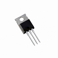
MOSFET N-CH 30V 38A TO-220AB

IRL3303

Manufacturer Part Number
IRL3303
Description
MOSFET N-CH 30V 38A TO-220AB
Manufacturer
International Rectifier
Series
HEXFET®r
Datasheet

Specifications of IRL3303

Fet Type
MOSFET N-Channel, Metal Oxide
Fet Feature
Logic Level Gate
Rds On (max) @ Id, Vgs
26 mOhm @ 20A, 10V
Drain To Source Voltage (vdss)
30V
Current - Continuous Drain (id) @ 25° C
38A
Vgs(th) (max) @ Id
1V @ 250µA
Gate Charge (qg) @ Vgs
26nC @ 4.5V
Input Capacitance (ciss) @ Vds
870pF @ 25V
Power - Max
68W
Mounting Type
Through Hole
Package / Case
TO-220-3 (Straight Leads)
Lead Free Status / RoHS Status
Contains lead / RoHS non-compliant
Other names
*IRL3303

Available stocks

Company
Part Number
Manufacturer
Quantity
Price
Part Number:
IRL3303
Manufacturer:
IR
Quantity:
15 171
Part Number:
IRL3303
Manufacturer:
IR
Quantity:
12 500
Company:
Part Number:
IRL3303
Quantity:
25 780
Part Number:
IRL3303LPBF
Manufacturer:
IR
Quantity:
21 400
Company:
Part Number:
IRL3303PBF
Quantity:
38
Part Number:
IRL3303S
Manufacturer:
IR
Quantity:
5 000
Part Number:
IRL3303SPBF
Manufacturer:
IR
Quantity:
21 400
Part Number:
IRL3303STBL
Manufacturer:
IR
Quantity:
20 000
Part Number:
IRL3303STRL
Manufacturer:
IR
Quantity:
20 000
Description
Absolute Maximum Ratings
Thermal Resistance
Fifth Generation HEXFETs from International Rectifier
utilize advanced processing techniques to achieve the
lowest possible on-resistance per silicon area. This benefit,
combined with the fast switching speed and ruggedized
device design that HEXFET Power MOSFETs are well
known for, provides the designer with an extremely efficient
device for use in a wide variety of applications.
The TO-220 package is universally preferred for all
commercial-industrial applications at power dissipation
levels to approximately 50 watts. The low thermal resistance
and low package cost of the TO-220 contribute to its wide
acceptance throughout the industry.
T
I
I
I
P
V
E
I
E
dv/dt
T
R
R
R
D
D
DM
AR
AS
J
STG
AR
D
GS
@ T
@ T
CS
JA
JC
@T
Logic-Level Gate Drive
Advanced Process Technology
Dynamic dv/dt Rating
175°C Operating Temperature
Fast Switching
Fully Avalanche Rated
C
C
C
= 25°C
= 100°C
= 25°C
Continuous Drain Current, V
Power Dissipation
Pulsed Drain Current
Linear Derating Factor
Gate-to-Source Voltage
Single Pulse Avalanche Energy
Avalanche Current
Repetitive Avalanche Energy
Peak Diode Recovery dv/dt
Operating Junction and
Storage Temperature Range
Soldering Temperature, for 10 seconds
Mounting torque, 6-32 or M3 screw.
Junction-to-Case
Case-to-Sink, Flat, Greased Surface
Junction-to-Ambient
Parameter
Parameter
GS
GS
@ 10V
@ 10V
G
Min.
––––
––––
––––
300 (1.6mm from case)
10 lbf•in (1.1N•m)
HEXFET
-55 to + 175
D
S
Typ.
––––
––––
0.50
Max.
0.45
140
±16
130
TO-220AB
6.8
5.0
38
27
68
20
®
R
IRL3303
Power MOSFET
DS(on)
Max.
––––
V
2.2
62
DSS
I
PD - 9.1322B
D
= 38A
= 0.026
= 30V
Units
Units
W/°C
°C/W
V/ns
mJ
mJ
°C
W
A
V
A
8/25/97

Related parts for IRL3303

IRL3303 Summary of contents

Page 1

... JC R Case-to-Sink, Flat, Greased Surface CS R Junction-to-Ambient 10V GS @ 10V GS 300 (1.6mm from case) Min. –––– –––– –––– 9.1322B IRL3303 ® HEXFET Power MOSFET 30V DSS R = 0.026 DS(on 38A D S TO-220AB Max. Units ...

Page 2

... IRL3303 Electrical Characteristics @ T Parameter V Drain-to-Source Breakdown Voltage (BR)DSS Breakdown Voltage Temp. Coefficient (BR)DSS J R Static Drain-to-Source On-Resistance DS(on) V Gate Threshold Voltage GS(th) g Forward Transconductance fs I Drain-to-Source Leakage Current DSS Gate-to-Source Forward Leakage I GSS Gate-to-Source Reverse Leakage Q Total Gate Charge g Q Gate-to-Source Charge ...

Page 3

... D S Fig 1. Typical Output Characteristics ° ° 0µ ate-to -S ource V olta Fig 3. Typical Transfer Characteristics A 10 100 = IRL3303 1000 VGS TOP 15V 12V 10V 8.0V 6.0V 4.0V 3.0V 100 BOTTOM 2. 0µ °C J 0.1 0 Drain-to-S ource Voltage ( Fig 2. Typical Output Characteristics ...

Page 4

... IRL3303 1600 1400 rss oss 1200 1000 800 600 C rss 400 200 rain-to-S ource Voltage ( Fig 5. Typical Capacitance Vs. Drain-to-Source Voltage ° ° ource-to-Drain Voltage ( Fig 7. Typical Source-Drain Diode Forward Voltage 100 20A TEST CIR CU IT SEE FIG otal Gate C harge ( Fig 6. Typical Gate Charge Vs. ...

Page 5

... RESPONSE) 0.01 0.00001 0.0001 Fig 11. Maximum Effective Transient Thermal Impedance, Junction-to-Case Fig 10a. Switching Time Test Circuit 125 150 175 ° Fig 10b. Switching Time Waveforms 0.001 t , Rectangular Pulse Duration (sec) 1 IRL3303 D.U. 4.5V Pulse Width µs Duty Factor V ...

Page 6

... IRL3303 4 Fig 12a. Unclamped Inductive Test Circuit Fig 12b. Unclamped Inductive Waveforms Charge Fig 13a. Basic Gate Charge Waveform L D.U. 0.01 V (BR)DSS V DD 300 250 200 150 100 100 125 Starting T , Junction T emperature (°C) J Fig 12c. Maximum Avalanche Energy Vs. Drain Current Current Regulator Same Type as D ...

Page 7

... Fig 14. For N-Channel HEXFETS Circuit Layout Considerations Low Stray Inductance Ground Plane Low Leakage Inductance Current Transformer - + dv/dt controlled Driver same type as D.U.T. I controlled by Duty Factor "D" SD D.U.T. - Device Under Test P. Period V GS Current di/dt Diode Recovery dv/ Forward Drop IRL3303 + =10V ...

Page 8

... IRL3303 Package Outline TO-220AB Outline Dimensions are shown in millimeters (inches (. (. & Part Marking Information TO-220AB 010 B1M WORLD HEADQUARTERS: 233 Kansas St., El Segundo, California 90245, Tel: (310) 322 3331 EUROPEAN HEADQUARTERS: Hurst Green, Oxted, Surrey RH8 9BB, UK Tel 1883 732020 IR CANADA: 7321 Victoria Park Ave., Suite 201, Markham, Ontario L3R 2Z8, Tel: (905) 475 1897 IR FAR EAST: K& ...

Page 9

Note: For the most current drawings please refer to the IR website at: http://www.irf.com/package/ ...

Related keywords