BUK7628-55A,118 NXP Semiconductors, BUK7628-55A,118 Datasheet - Page 2
BUK7628-55A,118
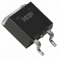
Manufacturer Part Number
BUK7628-55A,118
Description
MOSFET N-CH 55V 42A D2PAK
Manufacturer
NXP Semiconductors
Series
TrenchMOS™r
Datasheet
1.BUK7528-55A127.pdf
(9 pages)
Specifications of BUK7628-55A,118
Fet Type
MOSFET N-Channel, Metal Oxide
Fet Feature
Standard
Rds On (max) @ Id, Vgs
28 mOhm @ 25A, 10V
Drain To Source Voltage (vdss)
55V
Current - Continuous Drain (id) @ 25° C
42A
Vgs(th) (max) @ Id
4V @ 1mA
Input Capacitance (ciss) @ Vds
1165pF @ 25V
Power - Max
99W
Mounting Type
Surface Mount
Package / Case
D²Pak, TO-263 (2 leads + tab)
Configuration
Single
Transistor Polarity
N-Channel
Resistance Drain-source Rds (on)
0.028 Ohms
Drain-source Breakdown Voltage
55 V
Gate-source Breakdown Voltage
+/- 20 V
Continuous Drain Current
42 A
Power Dissipation
99 W
Maximum Operating Temperature
+ 175 C
Mounting Style
SMD/SMT
Minimum Operating Temperature
- 55 C
Lead Free Status / RoHS Status
Lead free / RoHS Compliant
Gate Charge (qg) @ Vgs
-
Lead Free Status / Rohs Status
Details
Other names
934056268118
BUK7628-55A /T3
BUK7628-55A /T3
BUK7628-55A /T3
BUK7628-55A /T3


Philips Semiconductors
STATIC CHARACTERISTICS
T
DYNAMIC CHARACTERISTICS
T
REVERSE DIODE LIMITING VALUES AND CHARACTERISTICS
T
June 2000
TrenchMOS
Standard level FET
j
SYMBOL PARAMETER
V
V
I
I
R
mb
SYMBOL PARAMETER
C
C
C
t
t
t
t
L
L
L
L
j
SYMBOL PARAMETER
I
I
V
t
Q
= 25˚C unless otherwise specified
DSS
GSS
d on
r
d off
f
DR
DRM
rr
= 25˚C unless otherwise specified
d
d
d
s
(BR)DSS
GS(TO)
SD
DS(ON)
iss
oss
rss
rr
= 25˚C unless otherwise specified
Drain-source breakdown
voltage
Gate threshold voltage
Zero gate voltage drain current
Gate source leakage current
Drain-source on-state
resistance
Input capacitance
Output capacitance
Feedback capacitance
Turn-on delay time
Turn-on rise time
Turn-off delay time
Turn-off fall time
Internal drain inductance
Internal drain inductance
Internal drain inductance
Internal source inductance
Continuous reverse drain
current
Pulsed reverse drain current
Diode forward voltage
Reverse recovery time
Reverse recovery charge
transistor
CONDITIONS
V
V
V
V
V
CONDITIONS
V
V
V
Measured from drain lead 6 mm
from package to centre of die
Measured from contact screw on
tab to centre of die(TO220AB)
Measured from upper edge of drain
tab to centre of die(SOT404)
Measured from source lead to
source bond pad
CONDITIONS
I
I
I
V
F
F
F
GS
DS
DS
GS
GS
GS
DD
GS
GS
= 25 A; V
= 41 A; V
= 20 A; -dI
= V
= 55 V; V
= 0 V; I
= 20 V; V
= 10 V; I
= 0 V; V
= 30 V; R
= 5 V; R
= -10 V; V
GS
; I
2
D
D
GS
GS
DS
G
D
F
= 0.25 mA;
= 1 mA
GS
/dt = 100 A/ s;
load
= 10
= 0 V
= 0 V
= 25 A
R
DS
= 25 V; f = 1 MHz
= 30 V
= 0 V;
=1.2 ;
= 0 V
T
T
T
T
T
j
j
j
j
j
= 175˚C
= 175˚C
= 175˚C
= -55˚C
= -55˚C
MIN.
MIN.
MIN.
55
50
2
1
-
-
-
-
-
-
-
-
-
-
-
-
-
-
-
-
-
-
-
-
-
-
-
TYP.
TYP.
TYP.
0.05
23.8
0.85
874
218
137
4.5
3.5
2.5
7.5
1.1
14
68
83
43
45
88
3
2
-
-
-
-
-
-
-
-
Product specification
BUK7528-55A
BUK7628-55A
MAX.
MAX.
MAX.
1165
500
100
261
188
102
116
163
4.4
1.2
10
28
56
21
60
41
50
96
4
-
-
-
-
-
-
-
-
Rev 1.100
UNIT
UNIT
UNIT
m
m
nH
nH
nH
nH
nC
nA
pF
pF
pF
ns
ns
ns
ns
ns
V
V
V
V
V
A
A
V
V
A
A
Related parts for BUK7628-55A,118
Image
Part Number
Description
Manufacturer
Datasheet
Request
R

Part Number:
Description:
Standard level N-channel enhancement mode Field-Effect Transistor (FET) in a plastic package using TrenchMOS technology
Manufacturer:
NXP Semiconductors
Datasheet:
Part Number:
Description:
Standard level N-channel enhancement mode Field-Effect Transistor (FET) in a plastic package using TrenchMOS technology
Manufacturer:
NXP Semiconductors
Datasheet:

Part Number:
Description:
MOSFET Power TAPE13 PWR-MOS
Manufacturer:
NXP Semiconductors

Part Number:
Description:
MOSFET N-CH 100V 47A SOT404
Manufacturer:
NXP Semiconductors
Datasheet:

Part Number:
Description:
MOSFET TAPE13 PWR-MOS
Manufacturer:
NXP Semiconductors
Datasheet:
Part Number:
Description:
MOSFET N-CH 100V SOT404
Manufacturer:
NXP Semiconductors
Datasheet:
Part Number:
Description:
NXP Semiconductors designed the LPC2420/2460 microcontroller around a 16-bit/32-bitARM7TDMI-S CPU core with real-time debug interfaces that include both JTAG andembedded trace
Manufacturer:
NXP Semiconductors
Datasheet:

Part Number:
Description:
NXP Semiconductors designed the LPC2458 microcontroller around a 16-bit/32-bitARM7TDMI-S CPU core with real-time debug interfaces that include both JTAG andembedded trace
Manufacturer:
NXP Semiconductors
Datasheet:
Part Number:
Description:
NXP Semiconductors designed the LPC2468 microcontroller around a 16-bit/32-bitARM7TDMI-S CPU core with real-time debug interfaces that include both JTAG andembedded trace
Manufacturer:
NXP Semiconductors
Datasheet:
Part Number:
Description:
NXP Semiconductors designed the LPC2470 microcontroller, powered by theARM7TDMI-S core, to be a highly integrated microcontroller for a wide range ofapplications that require advanced communications and high quality graphic displays
Manufacturer:
NXP Semiconductors
Datasheet:
Part Number:
Description:
NXP Semiconductors designed the LPC2478 microcontroller, powered by theARM7TDMI-S core, to be a highly integrated microcontroller for a wide range ofapplications that require advanced communications and high quality graphic displays
Manufacturer:
NXP Semiconductors
Datasheet:
Part Number:
Description:
The Philips Semiconductors XA (eXtended Architecture) family of 16-bit single-chip microcontrollers is powerful enough to easily handle the requirements of high performance embedded applications, yet inexpensive enough to compete in the market for hi
Manufacturer:
NXP Semiconductors
Datasheet:
Part Number:
Description:
The XA-S3 device is a member of Philips Semiconductors? XA(eXtended Architecture) family of high performance 16-bitsingle-chip microcontrollers
Manufacturer:
NXP Semiconductors
Datasheet:

Part Number:
Description:
The NXP BlueStreak LH75401/LH75411 family consists of two low-cost 16/32-bit System-on-Chip (SoC) devices
Manufacturer:
NXP Semiconductors
Datasheet: