IRF9620S Vishay, IRF9620S Datasheet - Page 5
IRF9620S
Manufacturer Part Number
IRF9620S
Description
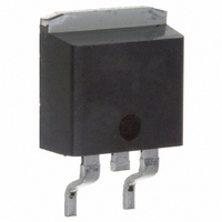
MOSFET P-CH 200V 3.5A D2PAK
Manufacturer
Vishay
Datasheet
1.IRF9620S.pdf
(7 pages)
Specifications of IRF9620S
Fet Type
MOSFET P-Channel, Metal Oxide
Fet Feature
Standard
Rds On (max) @ Id, Vgs
1.5 Ohm @ 1.5A, 10V
Drain To Source Voltage (vdss)
200V
Current - Continuous Drain (id) @ 25° C
3.5A
Vgs(th) (max) @ Id
4V @ 250µA
Gate Charge (qg) @ Vgs
22nC @ 10V
Input Capacitance (ciss) @ Vds
350pF @ 25V
Power - Max
3W
Mounting Type
Surface Mount
Package / Case
D²Pak, TO-263 (2 leads + tab)
Lead Free Status / RoHS Status
Contains lead / RoHS non-compliant
Other names
*IRF9620S
Available stocks
Company
Part Number
Manufacturer
Quantity
Price


Document Number: 91083
S09-0015-Rev. A, 19-Jan-09
91083_13
91083_14
91083_12
Fig. 13 - Maximum Drain Current vs. Case Temperature
Fig. 12 - Typical On-Resistance vs. Drain Current
3.5
3.0
2.5
2.0
1.5
1.0
0.5
0.0
40
35
30
25
20
15
10
Fig. 14 - Power vs. Temperature Derating Curve
2
5
0
4
1
5
3
0
25
0
0
R
pulse of 2.0 µs duration. Initial
T
2.0 µs pulse is minimal.)
J
DS(on)
=
25 °C. (Heating effect of
20
measured with current
- 4
50
T
T
C
C
40
, Case Temperature (°C)
, Case Temperature (°C)
I
D
, Drain Current (A)
- 8
75
60
V
GS
= - 10 V
80
- 12
100
100
V
GS
120
125
- 16
= - 20 V
140
150
- 20
V
GS
= - 10 V
Fig. 15 - Clamped Inductive Test Circuit
Fig. 16 - Clamped Inductive Waveforms
10 %
90 %
Fig. 17a - Switching Time Test Circuit
Fig. 17b - Switching Time Waveforms
Vary t
required I
V
V
GS
DS
R
t
p
Pulse width ≤ 1 µs
Duty factor ≤ 0.1 %
G
p
- 10 V
to obtain
V
IRF9620S, SiHF9620S
GS
t
L
d(on)
I
L
V
D.U.T.
DS
t
t
I
p
r
L
V
DD
= 0.5 V
D.U.T.
E
C
DS
R
Vishay Siliconix
D
t
d(off)
V
DS
E
V
DS
t
C
f
= 0.75 V
+
-
www.vishay.com
V
0.05 Ω
E
DD
V
C
V
DD
L
DD
DS
+
-
5
Related parts for IRF9620S
Image
Part Number
Description
Manufacturer
Datasheet
Request
R

Part Number:
Description:
357-036-542-201 CARDEDGE 36POS DL .156 BLK LOPRO
Manufacturer:
Vishay
Datasheet:
Part Number:
Description:
357-036-542-201 CARDEDGE 36POS DL .156 BLK LOPRO
Manufacturer:
Vishay
Datasheet:
Part Number:
Description:
357-036-542-201 CARDEDGE 36POS DL .156 BLK LOPRO
Manufacturer:
Vishay
Datasheet:
Part Number:
Description:
357-036-542-201 CARDEDGE 36POS DL .156 BLK LOPRO
Manufacturer:
Vishay
Datasheet:
Part Number:
Description:
357-036-542-201 CARDEDGE 36POS DL .156 BLK LOPRO
Manufacturer:
Vishay
Datasheet:
Part Number:
Description:
357-036-542-201 CARDEDGE 36POS DL .156 BLK LOPRO
Manufacturer:
Vishay
Datasheet:
Part Number:
Description:
357-036-542-201 CARDEDGE 36POS DL .156 BLK LOPRO
Manufacturer:
Vishay
Datasheet:
Part Number:
Description:
357-036-542-201 CARDEDGE 36POS DL .156 BLK LOPRO
Manufacturer:
Vishay
Datasheet:
Part Number:
Description:
357-036-542-201 CARDEDGE 36POS DL .156 BLK LOPRO
Manufacturer:
Vishay
Datasheet:
Part Number:
Description:
357-036-542-201 CARDEDGE 36POS DL .156 BLK LOPRO
Manufacturer:
Vishay
Datasheet:
Part Number:
Description:
357-036-542-201 CARDEDGE 36POS DL .156 BLK LOPRO
Manufacturer:
Vishay
Datasheet:
Part Number:
Description:
357-036-542-201 CARDEDGE 36POS DL .156 BLK LOPRO
Manufacturer:
Vishay
Datasheet:
Part Number:
Description:
357-036-542-201 CARDEDGE 36POS DL .156 BLK LOPRO
Manufacturer:
Vishay
Datasheet:
Part Number:
Description:
357-036-542-201 CARDEDGE 36POS DL .156 BLK LOPRO
Manufacturer:
Vishay
Datasheet:
Part Number:
Description:
357-036-542-201 CARDEDGE 36POS DL .156 BLK LOPRO
Manufacturer:
Vishay
Datasheet: