SPW52N50C3 Infineon Technologies, SPW52N50C3 Datasheet - Page 3
SPW52N50C3
Manufacturer Part Number
SPW52N50C3
Description
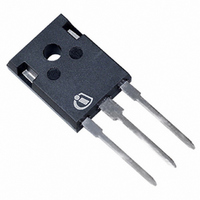
MOSFET N-CH 560V 52A TO-247
Manufacturer
Infineon Technologies
Series
CoolMOS™r
Specifications of SPW52N50C3
Package / Case
TO-247-3 (Straight Leads)
Fet Type
MOSFET N-Channel, Metal Oxide
Fet Feature
Standard
Rds On (max) @ Id, Vgs
70 mOhm @ 30A, 10V
Drain To Source Voltage (vdss)
560V
Current - Continuous Drain (id) @ 25° C
52A
Vgs(th) (max) @ Id
3.9V @ 2.7mA
Gate Charge (qg) @ Vgs
290nC @ 10V
Input Capacitance (ciss) @ Vds
6800pF @ 25V
Power - Max
417W
Mounting Type
Through Hole
Minimum Operating Temperature
- 55 C
Configuration
Single
Transistor Polarity
N-Channel
Resistance Drain-source Rds (on)
0.07 Ohm @ 10 V
Drain-source Breakdown Voltage
560 V
Gate-source Breakdown Voltage
+/- 20 V
Continuous Drain Current
52 A
Power Dissipation
417000 mW
Maximum Operating Temperature
+ 150 C
Mounting Style
Through Hole
Continuous Drain Current Id
52A
Drain Source Voltage Vds
560V
On Resistance Rds(on)
70mohm
Rds(on) Test Voltage Vgs
10V
Threshold Voltage Vgs Typ
3V
Rohs Compliant
Yes
Lead Free Status / RoHS Status
Lead free / RoHS Compliant
Lead Free Status / RoHS Status
Lead free / RoHS Compliant, Lead free / RoHS Compliant
Other names
SP000014626
SPW52N50C3
SPW52N50C3IN
SPW52N50C3X
SPW52N50C3XK
SPW52N50C3
SPW52N50C3IN
SPW52N50C3X
SPW52N50C3XK
Available stocks
Company
Part Number
Manufacturer
Quantity
Price
Company:

Part Number:
SPW52N50C3
Manufacturer:
INFINEON
Quantity:
149
Part Number:
SPW52N50C3
Manufacturer:
INFINEON/英飞凌
Quantity:
20 000


Please note the new package dimensions arccording to PCN 2009-134-A
Electrical Characteristics , at T
Parameter
Transconductance
Input capacitance
Output capacitance
Reverse transfer capacitance
Effective output capacitance,
energy related
Effective output capacitance,
time related
Turn-on delay time
Rise time
Turn-off delay time
Fall time
Gate Charge Characteristics
Gate to source charge
Gate to drain charge
Gate charge total
Gate plateau voltage
1 Repetitve avalanche causes additional power losses that can be calculated as P
2 C
3 C
4 I
Identical low-side and high-side switch.
Rev. 2.6
SD
o(er)
o(tr)
<=I
is a fixed capacitance that gives the same charging time as C
is a fixed capacitance that gives the same stored energy as C
D
, di/dt<=200A/us, V
DClink
=400V, V
2)
3)
g
C
C
C
C
C
t
t
t
t
Q
Q
Q
V
Symbol
d(on)
r
d(off)
f
j
fs
(plateau)
iss
oss
rss
o(er)
o(tr)
gs
gd
g
= 25 °C, unless otherwise specified
peak
<V
BR, DSS
V
I
V
f=1MHz
V
V
V
I
V
V
V
V
D
D
Page 3
DS
GS
GS
DS
DD
DD
DD
GS
DD
=30A
=52A, R
≥ 2* I
=0V to 400V
=380V, I
=380V, I
=0 to 10V
=380V, I
=0V, V
=0V,
=380V, V
Conditions
, T
D
j
* R
<T
G
DS
=1.8 Ω
DS(on)max
j,max
D
D
D
GS
=25V,
=52A
=52A,
=52A
=0/10V,
.
oss
oss
while V
while V
,
min.
DS
DS
-
-
-
-
-
-
-
-
-
-
-
-
-
-
AV
is rising from 0 to 80% V
is rising from 0 to 80% V
=E
Values
AR
6800
2200
212
469
typ.
150
120
160
290
*f.
30
40
20
30
10
5
SPW52N50C3
2008-02-11
max.
-
-
-
-
-
-
-
-
-
-
-
-
-
-
nC
V
Unit
S
pF
pF
ns
DSS
DSS
.
.
Related parts for SPW52N50C3
Image
Part Number
Description
Manufacturer
Datasheet
Request
R

Part Number:
Description:
Manufacturer:
Infineon Technologies AG
Datasheet:
Part Number:
Description:
Manufacturer:
Infineon Technologies AG
Datasheet:
Part Number:
Description:
Manufacturer:
Infineon Technologies AG
Datasheet:
Part Number:
Description:
Manufacturer:
Infineon Technologies AG
Datasheet:
Part Number:
Description:
Manufacturer:
Infineon Technologies AG
Datasheet:
Part Number:
Description:
Manufacturer:
Infineon Technologies AG
Datasheet:
Part Number:
Description:
Manufacturer:
Infineon Technologies AG
Datasheet:
Part Number:
Description:
16-bit microcontroller with 2x2 KByte RAM
Manufacturer:
Infineon Technologies AG
Datasheet:
Part Number:
Description:
NPN silicon RF transistor
Manufacturer:
Infineon Technologies AG
Datasheet:
Part Number:
Description:
NPN silicon RF transistor
Manufacturer:
Infineon Technologies AG
Datasheet:
Part Number:
Description:
NPN silicon RF transistor
Manufacturer:
Infineon Technologies AG
Datasheet:
Part Number:
Description:
NPN silicon RF transistor
Manufacturer:
Infineon Technologies AG
Datasheet:
Part Number:
Description:
Si-MMIC-amplifier in SIEGET 25-technologie
Manufacturer:
Infineon Technologies AG
Datasheet:
Part Number:
Description:
IGBT Power Module
Manufacturer:
Infineon Technologies AG
Datasheet:
Part Number:
Description:
IC for switching-mode power supplies
Manufacturer:
Infineon Technologies AG
Datasheet: