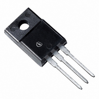
SPA04N50C3 Infineon Technologies, SPA04N50C3 Datasheet

SPA04N50C3
Specifications of SPA04N50C3
SPA04N50C3IN
SPA04N50C3X
SPA04N50C3XK
SPA04N50C3XTIN
SPA04N50C3XTIN
Available stocks
Related parts for SPA04N50C3
SPA04N50C3 Summary of contents
Page 1
Gate source voltage Power dissipation 25° Reverse diode dv/dt Rev. 2.9 SP000216298 T jmax E T ...
Page 2
wavesoldering Rev. 2.9 R thJC R thJA V (BR)DSS µ ...
Page 3
Transconductance Input capacitance Output capacitance Reverse transfer capacitance Turn-on delay time Rise time Turn-off delay time Fall time Gate to source charge Gate to drain charge 7 I <=I , di/dt<=400A/us DClink Identical low-side and high-side switch. ...
Page 4
Inverse diode direct current, pulsed Reverse recovery time Reverse recovery charge Peak reverse recovery current Rev rrm 2010-12-21 ...
Page 5
Rev. 2 tot 2010-12-21 ...
Page 6
Rev. 2 2010-12-21 3 ...
Page 7
Ω ≥ Rev. 2.9 Ω 2010-12-21 ...
Page 8
Rev. 2.9 ≤ (BR)DSS 2010-12-21 3 ...
Page 9
oss Rev. 2 2010-12-21 ...
Page 10
Rev. 2 2010-12-21 ...
Page 11
... PG-TO220-3-1, PG-TO220-3-21 Rev. 2.9 Page 11 SPP04N50C3 SPA04N50C3 2010-12-21 ...
Page 12
... PG-TO220-3-31 (FullPAK) Rev. 2.9 Page 12 SPP04N50C3 SPA04N50C3 2010-12-21 ...
Page 13
... Life support devices or systems are intended to be implanted in the human body or to support and/or maintain and sustain and/or protect human life. If they fail reasonable to assume that the health of the user or other persons may be endangered. Rev. 2.9 (www.infineon.com SPP04N50C3 SPA04N50C3 2010-12-21 ...


