NDF08N50ZG ON Semiconductor, NDF08N50ZG Datasheet
Home Discrete Semiconductor Products MOSFETs, GaNFETs - Single NDF08N50ZG
Manufacturer Part Number
NDF08N50ZG
Description
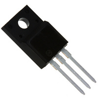
MOSFET N-CH 500V 7.5A TO-220FP
Manufacturer
ON Semiconductor
Specifications of NDF08N50ZG
Package / Case
TO-220-3 Full Pack (Straight Leads)
Mounting Type
Through Hole
Power - Max
31W
Fet Type
MOSFET N-Channel, Metal Oxide
Gate Charge (qg) @ Vgs
31nC @ 10V
Vgs(th) (max) @ Id
4.5V @ 100µA
Current - Continuous Drain (id) @ 25° C
7.5A
Drain To Source Voltage (vdss)
500V
Fet Feature
Standard
Rds On (max) @ Id, Vgs
850 mOhm @ 3.6A, 10V
Configuration
Single
Transistor Polarity
N-Channel
Resistance Drain-source Rds (on)
0.69 Ohms
Forward Transconductance Gfs (max / Min)
6 S
Drain-source Breakdown Voltage
500 V
Gate-source Breakdown Voltage
30 V
Continuous Drain Current
4.7 A
Power Dissipation
31 W
Maximum Operating Temperature
+ 125 C
Mounting Style
Through Hole
Gate Charge Qg
31 nC
Minimum Operating Temperature
- 55 C
Lead Free Status / RoHS Status
Lead free / RoHS Compliant
Available stocks
Manufacturer:
ON Semiconductor
NDF08N50Z, NDP08N50Z
N-Channel Power MOSFET
500 V, 0.69 W
Features
•
•
•
•
Stresses exceeding Maximum Ratings may damage the device. Maximum
Ratings are stress ratings only. Functional operation above the Recommended
Operating Conditions is not implied. Extended exposure to stresses above the
Recommended Operating Conditions may affect device reliability.
1. Limited by maximum junction temperature
2. I
ABSOLUTE MAXIMUM RATINGS
© Semiconductor Components Industries, LLC, 2010
April, 2010 − Rev. 1
Drain−to−Source Voltage
Continuous Drain Current
Continuous Drain Current
Pulsed Drain Current,
Power Dissipation
Gate−to−Source Voltage
Single Pulse Avalanche
ESD (HBM)
RMS Isolation Voltage
(t = 0.3 sec., R.H. ≤ 30%,
T
Peak Diode Recovery
Continuous Source
Maximum Temperature for
Operating Junction and
Storage Temperature Range
Low ON Resistance
Low Gate Charge
100% Avalanche Tested
These Devices are Pb−Free and are RoHS Compliant
A
SD
R
R
V
Energy, I
(JESD 22−A114)
Current (Body Diode)
Soldering Leads
= 25°C) (Figure 14)
GS
qJC
qJC
= 7.5 A, di/dt ≤ 100 A/ms, V
@ 10 V
T
A
Rating
= 100°C
D
= 7.5 A
Symbol
T
V
V
dv/dt
V
J
V
E
I
DD
P
T
, T
DSS
DM
I
I
ISO
I
esd
GS
D
D
AS
S
D
L
stg
≤ BV
(T
DSS
C
NDF08N50Z
7.5 (Note 1)
4.7 (Note 1)
30 (Note 1)
= 25°C unless otherwise noted)
, T
4500
31
J
= +150°C
−55 to 150
3500
500
190
260
4.5
7.5
30
NDP08N50Z
125
7.5
4.7
30
1
V/ns
Unit
mJ
°C
°C
W
V
A
A
A
V
V
V
A
NDF08N50ZG
NDP08N50ZG
Device
CASE 221D
CASE 221A
TO−220AB
TO−220FP
500 V
V
STYLE 1
STYLE 5
DSS
ORDERING INFORMATION
A
Y
WW
G
http://onsemi.com
TO−220FP
TO−220AB
Package
= Location Code
= Year
= Work Week
= Pb−Free Package
G (1)
Publication Order Number:
R
Gate
DS(ON)
NDF08N50ZG
NDP08N50ZG
MARKING
DIAGRAM
N−Channel
0.69 W
AYWW
(TYP) @ 3.6 A
Drain
In Development
D (2)
50 Units/Rail
or
NDF08N50Z/D
Shipping
Source
S (3)
Related parts for NDF08N50ZG
NDF08N50ZG Summary of contents
... G (1) TO−220FP CASE 221D MARKING STYLE 1 DIAGRAM NDF08N50ZG or NDP08N50ZG AYWW Gate TO−220AB CASE 221A STYLE 5 Drain A = Location Code Y = Year WW = Work Week G = Pb−Free Package ORDERING INFORMATION Device Package Shipping NDF08N50ZG TO−220FP 50 Units/Rail NDP08N50ZG TO−220AB In Development Publication Order Number: NDF08N50Z/D S (3) Source ...
THERMAL RESISTANCE Parameter Junction−to−Case (Drain) Junction−to−Ambient Steady State (Note 3) 3. Insertion mounted ELECTRICAL CHARACTERISTICS Characteristic OFF CHARACTERISTICS Drain−to−Source Breakdown Voltage Breakdown Voltage Temperature Coefficient Drain−to−Source Leakage Current Gate−to−Source Forward Leakage ON CHARACTERISTICS (Note 4) Static Drain−to−Source On−Resistance Gate Threshold ...
V 16.0 14 12.0 10.0 8.0 6.0 4.0 2.0 0.0 0.0 5.0 10.0 15 DRAIN−TO−SOURCE VOLTAGE (V) DS Figure 1. On−Region Characteristics 1.00 0.95 0.90 0.85 0.80 0.75 0.70 0.65 ...
T = 150° 125° 100 150 200 250 300 350 400 450 500 V , DRAIN−TO−SOURCE VOLTAGE (V) DS Figure 7. Drain−to−Source Leakage Current versus Voltage 15.0 14.0 13.0 12.0 11.0 ...
... Figure 13. Thermal Impedance (Junction−to−Case) for NDF08N50Z Measurement made between leads and heatsink with all leads shorted together. *For additional mounting information, please download the ON Semiconductor Soldering and Mounting Techniques Reference Manual, SOLDERRM/D. TYPICAL CHARACTERISTICS 100 ms ...
... Opportunity/Affirmative Action Employer. This literature is subject to all applicable copyright laws and is not for resale in any manner. PUBLICATION ORDERING INFORMATION LITERATURE FULFILLMENT: Literature Distribution Center for ON Semiconductor P.O. Box 5163, Denver, Colorado 80217 USA Phone: 303−675−2175 or 800−344−3860 Toll Free USA/Canada Fax: 303− ...
Related keywords
NDF08N50ZG datasheet NDF08N50ZG data sheet NDF08N50ZG pdf datasheet NDF08N50ZG component NDF08N50ZG part NDF08N50ZG distributor NDF08N50ZG RoHS NDF08N50ZG datasheet download