NTTFS4800NTWG ON Semiconductor, NTTFS4800NTWG Datasheet
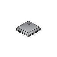
MOSFET N-CH 30V 5A 8WDFN

NTTFS4800NTWG

Manufacturer Part Number
NTTFS4800NTWG
Description
MOSFET N-CH 30V 5A 8WDFN
Manufacturer
ON Semiconductor
Datasheet

Specifications of NTTFS4800NTWG

Fet Type
MOSFET N-Channel, Metal Oxide
Fet Feature
Logic Level Gate
Rds On (max) @ Id, Vgs
20 mOhm @ 20A, 10V
Drain To Source Voltage (vdss)
30V
Current - Continuous Drain (id) @ 25° C
5A
Vgs(th) (max) @ Id
3V @ 250µA
Gate Charge (qg) @ Vgs
16.6nC @ 10V
Input Capacitance (ciss) @ Vds
964pF @ 15V
Power - Max
860mW
Mounting Type
Surface Mount
Package / Case
8-WDFN
Configuration
Single
Transistor Polarity
N-Channel
Resistance Drain-source Rds (on)
11.1 Ohms
Forward Transconductance Gfs (max / Min)
28 S
Drain-source Breakdown Voltage
30 V
Gate-source Breakdown Voltage
20 V
Continuous Drain Current
8.3 A
Power Dissipation
2.2 W
Maximum Operating Temperature
+ 125 C
Mounting Style
SMD/SMT
Gate Charge Qg
8.4 nC
Minimum Operating Temperature
- 55 C
Lead Free Status / RoHS Status
Lead free / RoHS Compliant
NTTFS4800N
Power MOSFET
30 V, 32 A, Single N−Channel, m8FL
Features
Applications
Stresses exceeding Maximum Ratings may damage the device. Maximum
Ratings are stress ratings only. Functional operation above the Recommended
Operating Conditions is not implied. Extended exposure to stresses above the
Recommended Operating Conditions may affect device reliability.
1. Surface−mounted on FR4 board using 1 sq−in pad, 1 oz Cu.
2. Surface−mounted on FR4 board using the minimum recommended pad size.
© Semiconductor Components Industries, LLC, 2011
January, 2011 − Rev. 1
MAXIMUM RATINGS
Drain−to−Source Voltage
Gate−to−Source Voltage
Continuous Drain
Current R
Power Dissipation R
(Note 1)
Continuous Drain
Current R
(Note 1)
Power Dissipation
R
Continuous Drain
Current R
Power Dissipation
R
Continuous Drain
Current R
Power Dissipation
R
Pulsed Drain Current
Operating Junction and Storage Temperature
Source Current (Body Diode)
Drain to Source DV/DT
Single Pulse Drain−to−Source Avalanche Energy
(T
I
Lead Temperature for Soldering Purposes
(1/8″ from case for 10 s)
L
Compliant
Low R
Low Capacitance to Minimize Driver Losses
Optimized Gate Charge to Minimize Switching Losses
These Devices are Pb−Free, Halogen Free/BFR Free and are RoHS
DC−DC Converters
Point of Load
Power Load Switch
Notebook Battery Management
Motor Control
qJA
qJA
qJC
J
= 27 A
= 25°C, V
≤ 10 s (Note 1)
(Note 2)
(Note 1)
pk
DS(on)
qJA
qJA
qJA
qJC
, L = 0.1 mH, R
DD
(Note 1)
≤ 10 s
(Note 2)
(Note 1)
to Minimize Conduction Losses
= 50 V, V
Parameter
qJA
(T
GS
G
J
Steady
T
State
= 25 W)
= 25°C unless otherwise stated)
A
= 10 V,
= 25°C, t
T
T
T
T
T
T
T
T
T
T
T
T
p
A
A
A
A
A
A
A
A
A
C
C
C
= 10 ms
= 25°C
= 85°C
= 25°C
= 25°C
= 85°C
= 25°C
= 25°C
= 85°C
= 25°C
= 25°C
= 85°C
= 25°C
Symbol
V
dV/dt
V
E
T
I
T
P
P
P
P
DSS
T
I
I
I
I
DM
I
stg
GS
AS
D
D
D
D
S
J
D
D
D
D
L
,
−55 to
Value
+150
11.8
0.86
33.8
36.6
±20
260
8.3
6.0
2.2
8.5
4.5
5.0
3.6
6.0
30
32
23
57
28
1
V/ns
Unit
mJ
°C
°C
W
W
W
W
V
V
A
A
A
A
A
A
†For information on tape and reel specifications,
NTTFS4800NTAG
NTTFS4800NTWG
including part orientation and tape sizes, please
refer to our Tape and Reel Packaging Specification
Brochure, BRD8011/D.
V
CASE 511AB
(BR)DSS
30 V
(Note: Microdot may be in either location)
Device
WDFN8
(m8FL)
ORDERING INFORMATION
4800
A
Y
WW
G
G (4)
1
http://onsemi.com
N−Channel MOSFET
27 mW @ 4.5 V
20 mW @ 10 V
R
= Specific Device Code
= Assembly Location
= Year
= Work Week
= Pb−Free Package
D (5−8)
DS(on)
(Pb−Free)
(Pb−Free)
Package
WDFN8
WDFN8
MARKING DIAGRAM
Publication Order Number:
G
S
S
S
MAX
1
S (1,2,3)
AYWWG
1500/Tape & Reel
5000/Tape & Reel
4800
NTTFS4800N/D
G
Shipping
I
D
32 A
MAX
D
D
D
D

Related parts for NTTFS4800NTWG

NTTFS4800NTWG Summary of contents

Page 1

... P 33 Device T , −55 to °C J NTTFS4800NTAG T +150 stg NTTFS4800NTWG dV/dt 6.0 V/ †For information on tape and reel specifications, including part orientation and tape sizes, please refer to our Tape and Reel Packaging Specification T 260 °C Brochure, BRD8011/ http://onsemi.com R MAX I MAX DS(on) ...

Page 2

THERMAL RESISTANCE MAXIMUM RATINGS Parameter Junction−to−Case (Drain) Junction−to−Ambient – Steady State (Note 3) Junction−to−Ambient – Steady State (Note 4) Junction−to−Ambient – (t ≤ (Note 3) 3. Surface−mounted on FR4 board using 1 sq−in pad Cu. 4. ...

Page 3

ELECTRICAL CHARACTERISTICS (T Parameter SWITCHING CHARACTERISTICS (Note 6) Turn−On Delay Time Rise Time Turn−Off Delay Time Fall Time DRAIN−SOURCE DIODE CHARACTERISTICS Forward Diode Voltage Reverse Recovery Time Charge Time Discharge Time Reverse Recovery Charge PACKAGE PARASITIC VALUES Source Inductance Drain ...

Page 4

V 4 4 0 DRAIN−TO−SOURCE VOLTAGE (V) DS Figure 1. On−Region Characteristics 0.030 0.028 0.026 0.024 0.022 0.020 0.018 0.016 0.014 0.012 ...

Page 5

C iss 1000 800 600 400 C oss 200 C rss DRAIN−TO−SOURCE VOLTAGE (V) DS Figure 7. Capacitance Variation 100 ...

Page 6

Duty Cycle = 50% 100 20 0.1 Single Pulse 0.01 0.000001 0.00001 0.0001 TYPICAL CHARACTERISTICS 0.001 0.01 0.1 PULSE TIME (sec) Figure 13. Thermal Response http://onsemi.com 100 1000 ...

Page 7

... M 0.57 0.75 0.47 *For additional information on our Pb−Free strategy and soldering details, please download the ON Semiconductor Soldering and Mounting Techniques Reference Manual, SOLDERRM/D. N. American Technical Support: 800−282−9855 Toll Free USA/Canada Europe, Middle East and Africa Technical Support: Phone: 421 33 790 2910 Japan Customer Focus Center Phone: 81− ...

Related keywords