NTD25P03LT4G ON Semiconductor, NTD25P03LT4G Datasheet

MOSFET P-CH 30V 25A DPAK

NTD25P03LT4G

Manufacturer Part Number
NTD25P03LT4G
Description
MOSFET P-CH 30V 25A DPAK
Manufacturer
ON Semiconductor
Datasheet

Specifications of NTD25P03LT4G

Fet Type
MOSFET P-Channel, Metal Oxide
Fet Feature
Logic Level Gate
Rds On (max) @ Id, Vgs
80 mOhm @ 25A, 5V
Drain To Source Voltage (vdss)
30V
Current - Continuous Drain (id) @ 25° C
25A
Vgs(th) (max) @ Id
2V @ 250µA
Gate Charge (qg) @ Vgs
20nC @ 5V
Input Capacitance (ciss) @ Vds
1260pF @ 25V
Power - Max
75W
Mounting Type
Surface Mount
Package / Case
DPak, TO-252 (2 leads+tab), SC-63
Configuration
Single
Transistor Polarity
P-Channel
Resistance Drain-source Rds (on)
0.051 Ohms
Forward Transconductance Gfs (max / Min)
13 S
Drain-source Breakdown Voltage
- 30 V
Gate-source Breakdown Voltage
+/- 15 V
Continuous Drain Current
- 25 A
Power Dissipation
75 W
Maximum Operating Temperature
+ 150 C
Mounting Style
SMD/SMT
Minimum Operating Temperature
- 55 C
Lead Free Status / RoHS Status
Lead free / RoHS Compliant
Other names
NTD25P03LT4GOS
NTD25P03LT4GOS
NTD25P03LT4GOSTR

Available stocks

Company
Part Number
Manufacturer
Quantity
Price
Part Number:
NTD25P03LT4G
Manufacturer:
ON
Quantity:
15 000
Part Number:
NTD25P03LT4G
Manufacturer:
ON
Quantity:
12 500
Part Number:
NTD25P03LT4G
Manufacturer:
ON/安森美
Quantity:
20 000
Part Number:
NTD25P03LT4G
0
Company:
Part Number:
NTD25P03LT4G
Quantity:
4 500
NTD25P03L
Power MOSFET
−25 Amp, −30 Volt
Logic Level P−Channel DPAK
withstand high energy in the avalanche and commutation modes. The
source−to−drain diode recovery time is comparable to a discrete fast
recovery diode.
Features
Typical Applications
Stresses exceeding Maximum Ratings may damage the device. Maximum
Ratings are stress ratings only. Functional operation above the Recommended
Operating Conditions is not implied. Extended exposure to stresses above the
Recommended Operating Conditions may affect device reliability.
1. When surface mounted to an FR4 board using 0.5 sq in pad size.
2. When surface mounted to an FR4 board using the minimum recommended
MAXIMUM RATINGS
© Semiconductor Components Industries, LLC, 2006
March, 2006 − Rev. 3
Drain−to−Source Voltage
Gate−to−Source Voltage
Drain Current
Total Power Dissipation @ T
Operating and Storage Temperature Range
Single Pulse Drain−to−Source Avalanche
Energy − Starting T
(V
Peak I
Thermal Resistance
Maximum Lead Temperature for Soldering
Purposes, (1/8 in from case for 10 seconds)
Designed for low voltage, high speed switching applications and to
Pb−Free Packages are Available
PWM Motor Controls
Power Supplies
Converters
Bridge Circuits
pad size.
DD
− Continuous
− Non−Repetitive (tp ≤ 10 ms)
− Continuous @ T
− Single Pulse (t
− Junction−to−Case
− Junction−to−Ambient (Note 1)
− Junction−to−Ambient (Note 2)
= 25 Vdc, V
L
= 20 Apk, L = 1.0 mH, R
GS
Rating
J
p
= 5.0 Vdc,
= 25°C
A
≤ 10 ms)
= 25°C
(T
J
= 25°C unless otherwise noted)
A
= 25°C
G
= 25 W)
Symbol
T
V
V
R
R
R
J
V
E
I
GSM
P
, T
DSS
T
I
DM
qJC
qJA
qJA
GS
AS
D
D
L
stg
−55 to
Value
+150
"15
"20
1.65
−30
−25
−75
200
120
260
75
67
1
°C/W
Unit
Vpk
Apk
mJ
°C
°C
W
V
V
A
1 2
See detailed ordering and shipping information in the package
dimensions section on page 7 of this data sheet.
1
V
2
(BR)DSS
−30 V
3
3
Y
WW
25P03L
G
ORDERING INFORMATION
4
4
G
http://onsemi.com
CASE 369C
CASE 369D
51 mW @ 5.0 V
STYLE 2
STYLE 2
DPAK−3
R
P−Channel
DPAK
DS(on)
D
= Year
= Work Week
= Device Code
= Pb−Free Package
MARKING DIAGRAMS
Publication Order Number:
& PIN ASSIGNMENTS
S
Typ
Gate
Gate
1
1
NTD25P03L/D
Drain
Drain
Drain
Drain
4
2
4
2
I
D
−25 A
Max
3
Source
3
Source

Related parts for NTD25P03LT4G

NTD25P03LT4G Summary of contents

Page 1

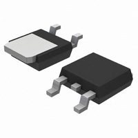
NTD25P03L Power MOSFET −25 Amp, −30 Volt Logic Level P−Channel DPAK Designed for low voltage, high speed switching applications and to withstand high energy in the avalanche and commutation modes. The source−to−drain diode recovery time is comparable to a discrete ...

Page 2

ELECTRICAL CHARACTERISTICS Characteristic OFF CHARACTERISTICS Drain−to−Source Breakdown Voltage (Note Vdc −250 mA Temperature Coefficient (Positive) Zero Gate Voltage Drain Current (V = −30 Vdc Vdc 25°C) DS ...

Page 3

TYPICAL MOSFET ELECTRICAL CHARACTERISTICS −V , DRAIN−TO−SOURCE VOLTAGE (VOLTS) DS Figure 1. On−Region Characteristics 0 ...

Page 4

Switching behavior is most easily modeled and predicted by recognizing that the power MOSFET is charge controlled. The lengths of various switching intervals (Dt) are determined by how fast the FET input capacitance can be charged by current from the ...

Page 5

... RR Compared to ON Semiconductor standard cell density low voltage MOSFETs, high cell density MOSFET diodes are faster (shorter t reverse recovery characteristic. The softness advantage of the high cell density diode means they can be forced through ...

Page 6

The Forward Biased Safe Operating Area curves define the maximum simultaneous drain−to−source voltage and drain current that a transistor can handle safely when it is forward biased. Curves are based upon maximum peak junction temperature and a case temperature (T ...

Page 7

... Figure 14. Diode Reverse Recovery Waveform ORDERING INFORMATION Device NTD25P03L NTD25P03LG NTD25P03L1 NTD25P03L1G NTD25P03LT4 NTD25P03LT4G NTD25P03LRL NTD25P03LRLG †For information on tape and reel specifications, including part orientation and tape sizes, please refer to our Tape and Reel Packaging Specifications Brochure, BRD8011/D. P (pk ...

Page 8

... 0.13 (0.005) M 5.80 0.228 *For additional information on our Pb−Free strategy and soldering details, please download the ON Semiconductor Soldering and Mounting Techniques Reference Manual, SOLDERRM/D. PACKAGE DIMENSIONS DPAK CASE 369C−01 ISSUE O SEATING −T− PLANE SOLDERING FOOTPRINT* 6.20 3.0 0.244 0.118 2 ...

Page 9

... American Technical Support: 800−282−9855 Toll Free USA/Canada Japan: ON Semiconductor, Japan Customer Focus Center 2−9−1 Kamimeguro, Meguro−ku, Tokyo, Japan 153−0051 Phone: 81−3−5773−3850 http://onsemi.com 9 NOTES: 1. DIMENSIONING AND TOLERANCING PER ANSI Y14.5M, 1982. 2. CONTROLLING DIMENSION: INCH. ...

Related keywords